11 Hardware Acceleration
Purpose
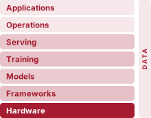
Architecture stack focus for this chapter.
Why does moving data cost more than computing it?
Arithmetic is inexpensive relative to data movement. In the time required to fetch a single scalar operand from off-chip DRAM, modern arithmetic units can execute dozens to hundreds of floating-point operations, and that DRAM access consumes on the order of a hundred times more energy than the computation itself. This fundamental imbalance, the memory wall, means specialized accelerators are not merely faster arithmetic engines. Rather, their microarchitectures are designed to stage, amortize, and hide data movement through wide spatial interconnects, deep on-chip memory hierarchies, and specialized execution pipelines. When general-purpose processor scaling faltered, hardware specialization enabled machine learning models to continue scaling by turning transistor budgets into high-throughput tensor datapaths. Delivered performance, however, depends on whether a model’s tensor access patterns match the data paths of the underlying silicon. Hardware selection cannot be reduced to comparing peak FLOP/s: two accelerators with identical theoretical compute ratings often deliver radically different throughput on real workloads because one saturates its functional units while the other starves for data. A recommendation model dominated by sparse embedding lookups stresses memory bandwidth and interconnect latency, demanding a fundamentally different memory architecture than a dense transformer training run bounded by matrix multiply-accumulate throughput. If an operation is bandwidth bound, reducing theoretical operation count yields zero speedup because arithmetic is not the binding constraint. Matching workload characteristics to architectural dataflows determines whether an accelerator operates near its hardware ceiling or languishes at a fraction of its advertised peak. In D·A·M terms, the accelerator makes the machine constraint concrete, governing which algorithms and model architectures remain practical in production.
Learning Objectives
- Explain hardware acceleration as tensor-workload specialization and why Amdahl’s law bounds its end-to-end speedup
- Compare Tensor Cores, systolic arrays, SIMD/SIMT units, and sparse execution for ML compute primitives
- Diagnose memory-wall bottlenecks using bandwidth, cache hierarchy, host-device transfer, and energy-movement costs
- Calculate arithmetic intensity and execution-path roofline ceilings, then use profiling to diagnose compute or memory limits
- Select dataflow, tiling, and mapping strategies that maximize reuse under memory-capacity constraints
- Analyze compiler and runtime optimizations that fuse kernels, plan memory, and schedule accelerators
- Evaluate accelerator choices across throughput, latency, power, cost, and deployment-context constraints
11.1 Anatomy of an Accelerator

Hardware acceleration turns on the machine axis.
Model Compression closed on a deployment profile for ResNet-50 quantized to INT8 (ResNet-50 INT8 Deployment Profile on the Reference H100): a model four times smaller whose large-batch throughput rises severalfold on the reference H100 while its batch-one latency barely moves. Data selection reduced the iron law’s Data factor (\(\text{Samples/Task}\)) and compression reduced the Algorithm factor (\(\text{FLOPs/Sample}\)) and byte traffic (\(\DataVolume\)), but whether either saving reaches the wall clock is decided by the Machine factor (\(\text{Seconds/FLOP}\)). This chapter supplies the machine side of that profile. It explains why the same INT8 weights run faster on one execution path than on another, and why the hardware, not the model, determines how much of every compression saving survives execution. The explanation starts with the memory wall: arithmetic is cheap relative to data movement, so specialized hardware matters less because it raises compute throughput than because it organizes memory, dataflow, and parallelism so that its arithmetic units stay fed.
One workload runs through the chapter. ResNet-50 quantized to INT8 carries the book’s compute-bound regime (Lighthouse Models as Reference Workloads): its convolutions reuse each weight across many image positions, so on a data-center accelerator most of its time can go to arithmetic rather than to moving bytes. It reappears at every level of the machine, from the matrix units that execute its convolutions to the compiler that lowers its graph, and each time the question is what the INT8 path changes. GPT-2 XL decoding one token at a time supplies the single contrast. It carries the bandwidth-bound regime: every generated token streams all of the model’s weights from memory for about two operations per parameter, so the machine that keeps ResNet-50 busy spends most of a decode step waiting for bytes. MobileNetV2, whose depthwise layers trade arithmetic for a small parameter footprint, and keyword spotting (KWS), the power-bound lighthouse, return where the chapter reaches phone-class and embedded chips. DLRM appears where its embedding lookups, the capacity-bound regime, break the regular access patterns that accelerators assume. The reference machine is the NVIDIA H100, the data-center accelerator this book uses for training and serving examples; its numbers are one generation’s instance of limits that every generation obeys.
Definition 11.1: Hardware acceleration
Hardware acceleration is the practice of mapping work from general-purpose execution onto specialized processors or functional units optimized for a narrower operation class. For ML workloads, that specialization commonly trades some programmability for the compute density \((\PeakRate)\) and performance-per-watt gains that regular tensor operations can exploit.
- Significance: An H100 GPU delivers 989 TFLOP/s for dense FP16/BF16 matrix multiplication; against this chapter’s illustrative 1–2 TFLOP/s reference-CPU baseline, this is a 490–990× gap. Its 80 billion transistors devote far more silicon to parallel arithmetic than to branch prediction, out-of-order scheduling, and large caches (Choquette 2023).
- Distinction: A general-purpose CPU is designed for flexible execution, low-latency control, and varied workloads. An accelerator instead concentrates resources on a narrower operation class, so it achieves its gains only when the workload exposes the supported operations and enough parallel work to keep its arithmetic units busy.
- Common pitfall: A frequent misconception is that an accelerator’s advertised peak throughput is the throughput a workload receives. Delivered performance is bounded above by the lower of the compute ceiling and what memory bandwidth can feed (the roofline constraint, developed later in this chapter), so a low-arithmetic-intensity kernel can sit at a small fraction of peak FLOP/s no matter how fast the silicon is rated, because it starves for data rather than for arithmetic.
The anatomy of an accelerator is the arrangement of parts that every machine learning accelerator shares: arithmetic units built for tensor operations, on-chip memory that holds operands next to those units, a wide path to off-chip memory, and a host interface through which work arrives. Every inference and every training step on such a machine is a stream of operand movements that ends in multiply-accumulate operations, and the anatomy decides how far each operand travels before it is used. A matrix unit that can retire thousands of multiply-accumulates per cycle sits idle whenever its next operands are still in flight, and an off-chip access can take many processor cycles and cost orders of magnitude more energy than the low-precision operation it feeds. The arithmetic units are the easy part of the design; the rest of the anatomy exists to keep them fed.
The definition becomes concrete in the generic chip of figure 1, which serves as this chapter’s map. External high-bandwidth memory (HBM) feeds shared on-chip storage (an L2 cache), which distributes operands into rows of processing elements, each equipped with a private scratchpad or cache, a matrix unit, a vector unit, and a special function unit. A host interface connects the chip to the CPU that issues its work.
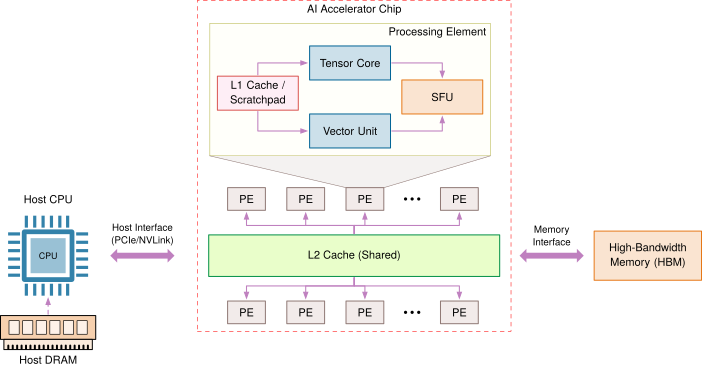
Within each processing element, specialized units partition execution across distinct mathematical primitives: dedicated matrix units (Tensor Cores) execute dense matrix multiplication, vector units evaluate element-wise arithmetic, and special function units (SFUs) approximate transcendental operations such as activations and exponentials. Their number, grouping, and names vary by vendor; some designs arrange them into an explicit 2D systolic grid, and others distribute matrix engines among wide parallel cores.
The memory hierarchy amortizes the cost of data transport across tiers. High-bandwidth memory provides off-chip capacity and throughput, while shared on-chip storage and per-element caches or scratchpads cut off-chip traffic. Because moving a tensor tile across the package boundary costs orders of magnitude more energy than keeping it on chip, compilers and kernels must coordinate tile capacity, reuse, and prefetching to keep operands staged locally; more HBM bandwidth raises the off-chip ceiling, but without local reuse the execution units still stall. The system assumptions appendix (System Assumptions) collects reference specifications for the accelerators this book uses, including the H100.
The host interface links the accelerator to the host CPU, which coordinates execution graphs, asynchronous I/O, and fallback operations while the accelerator executes dispatched kernels. Direct-memory-access engines can overlap host-device transfers with execution, but an operator unsupported by the accelerator backend may require a CPU round-trip. An operator outside the matrix-unit instruction set may instead use vector or other device kernels. These execution boundaries help set the effective speedup envelope. Kernel execution time matters little if transfers, launches, and synchronization dominate end-to-end latency. The three parts of the figure (the processing elements, the memory tiers, and the host link) are the parts this chapter takes apart in turn.
The anatomy embodies the chapter’s central engineering trade-off. General-purpose processors allocate silicon area to complex control logic, speculative execution, branch prediction, and multi-level cache hierarchies to handle arbitrary control flow. An accelerator redirects that transistor budget toward dense arithmetic arrays, dedicated register files, and high-bandwidth memory paths tailored to a narrower workload class. When the software path exposes sufficient tensor parallelism, this specialization yields order-of-magnitude improvements in energy efficiency and throughput per watt. Silicon built for a narrow class of dense tensor operations pays off only because, as the bitter lesson predicts, the general methods that win by exploiting computation keep reducing to those same operations at ever larger scale. The dependence also runs the other way, because scale keeps winning only while accelerators keep lowering the time and energy of each additional operation, so the hardware this chapter studies is part of what sustains the bitter lesson itself.
↩︎ The bitter lesson, the observation that general methods exploiting computation win as computation grows, is established in The Bitter Lesson.
Hardware alone cannot achieve these gains. Algorithms must structure operations to expose data reuse and regular memory access, while silicon architectures must allocate physical units to the mathematical primitives and numeric precisions that algorithms actually execute. That mutual dependence motivates a complementary principle: hardware-software co-design.
Definition 11.2: Hardware-software co-design
Hardware-Software Co-design is an ML accelerator development method that crosses conventional abstraction boundaries, allowing algorithm constraints to inform silicon design and hardware capabilities to shape algorithm formulation.
- Significance: On a supported tensor-core path, 8-bit integer (INT8) quantization can deliver multi-fold throughput gains because hardware executes lower-precision operations more densely and moves fewer bytes than an FP32 path; the exact gain depends on the architecture and workload (NVIDIA Corporation 2020a; Dally et al. 2021; Dally 2023).
- Distinction: Unlike layered abstraction (where software calls a hardware API without knowing the silicon details), co-design exposes hardware constraints directly to algorithm and compiler authors: data alignment requirements, precision formats, and memory access patterns all become visible inputs to global cross-layer optimization.
- Common pitfall: A frequent misconception is that co-design is a one-time hardware design choice. In practice, the supported features continue to evolve: NVIDIA Tensor Cores began with FP16 matrix multiplication, later generations added TF32 and broader integer support, and Ampere added acceleration for 2:4 structured sparsity (NVIDIA 2017; NVIDIA Corporation 2020a).
Co-design explains why model compression techniques deliver real speedups. Quantization shows why converting FP32 to INT8 accelerates execution on supported hardware: reduced precision cuts memory traffic, while specialized arithmetic units execute more low-precision operations per cycle than FP32 equivalents (NVIDIA Corporation 2020a). Structured pruning improves performance when it produces smaller dense shapes or a sparsity pattern recognized by silicon, whereas arbitrary unstructured sparsity incurs metadata handling and non-coalesced memory accesses that often erase theoretical gains. Evaluating accelerator performance requires tracing this path from workload to silicon: compute primitives, memory hierarchies, roofline diagnosis, mapping and dataflow, and compiler scheduling. The recurring question is why algorithmic improvements frequently fail to deliver proportional end-to-end speedups. Amdahl’s law (principle 8) already answered it for model-side optimizations, since whatever an optimization leaves untouched caps the overall gain. The same bound governs hardware. The theorem below applies the principle to an accelerator, and the only new quantity is the gain, which becomes the accelerator’s path gain \(\AcceleratorGain\).
↩︎ Quantization and its effect on weight payload, memory traffic, and compute cost are established in Numerical Precision: Changing How Values Are Stored.
Theorem 11.1: The fundamental limit of acceleration (Amdahl's law)
Hardware acceleration does not speed up the entire system; it speeds only the baseline-time fraction using the accelerated path. For that fraction \(\ParallelFraction\) and path gain \(\AcceleratorGain\), Amdahl’s law (Amdahl 1967) gives the bound in equation 1. \[ \text{Speedup} = \frac{1}{(1 - \ParallelFraction) + \frac{\ParallelFraction}{\AcceleratorGain}} \tag{1}\]
- Accelerated fraction (\(\ParallelFraction\)): Share of baseline time receiving the stated gain, often in matrix multiplication or another supported kernel.
- Accelerator gain (\(\AcceleratorGain\)): The raw speed advantage of the GPU or Tensor Processing Unit (TPU) over the CPU for the accelerated portion of the workload.
- Unaccelerated fraction (\(1-\ParallelFraction\)): Work outside the chosen path, such as data loading, host overhead, unsupported operators, and kernel launch latency.
Pitfall: Unaccelerated work caps total speedup. If 10 percent of baseline time is unaffected (\(\ParallelFraction=0.9\)), even infinite path gain (\(\AcceleratorGain=\infty\)) yields at most 10\(\times\) overall. Once the accelerated component is fast enough, unaffected work dominates.
Amdahl, Gene M. 1967. “Validity of the Single Processor Approach to Achieving Large Scale Computing Capabilities.” Proceedings of the April 18-20, 1967, Spring Joint Computer Conference on - AFIPS ’67 (Spring), AFIPS ’67 (spring), 483–85. https://doi.org/10.1145/1465482.1465560.
1 Amdahl’s law: Maps onto the iron law only after the proposed change is specified. If a faster tensor unit reduces the computation term \((\Operations/(\PeakRate \cdot \EfficiencyHw))\) but leaves data transfer and fixed latency unchanged, those unaffected terms bound total speedup. A different accelerator or memory system may improve bandwidth as well. The unaccelerated fraction is therefore defined by the intervention, not by a permanent classification of each term as serial.
Hardware acceleration targets specific terms in the iron law of ML systems, which decomposes end-to-end time into data movement \((\DataVolume/\Bandwidth)\), computation \((\Operations/(\PeakRate \cdot \EfficiencyHw))\), and fixed latency \((\Latency)\). While data selection reduced the number of samples processed (\(\text{Samples/Task}\), shrinking both \(\Operations\) and input traffic \(\DataVolume\)) and model compression reduced the operations and bytes per sample (\(\text{FLOPs/Sample}\) and weight traffic \(\DataVolume\)), hardware acceleration reduces the realized time per operation (\(\text{Seconds/FLOP}\)) by improving \(\PeakRate\), \(\EfficiencyHw\), and \(\Bandwidth\). Which of these physical terms an upgrade actually improves determines its accelerated fraction under Amdahl’s law.1
↩︎ The decomposition of execution time into data, compute, and latency terms is established in Iron Law of ML Systems.
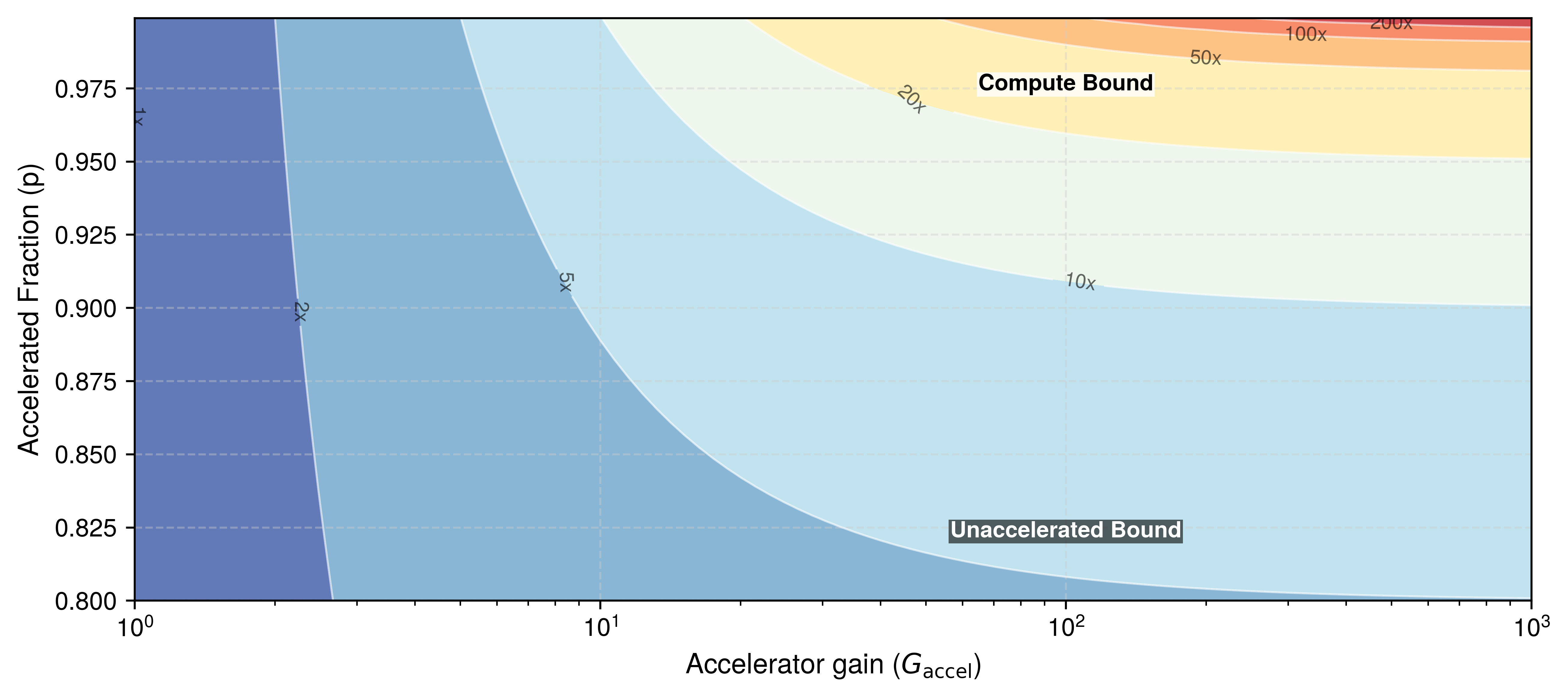
This dynamic explains why hardware upgrades frequently fail to produce proportional end-to-end speedups. Figure 2 maps system speedup across accelerator gain (\(\AcceleratorGain\)) and accelerated fraction (\(\ParallelFraction\)), charting where those returns diminish. Where the unaccelerated fraction \(1-\ParallelFraction\) remains substantial, the white contour curves flatten horizontally into the unaccelerated-bound regime, bounding total speedup at the \(1/(1-\ParallelFraction)\) asymptote regardless of how far \(\AcceleratorGain\) scales along the horizontal axis. Because \(\ParallelFraction\) differs substantially across workload archetypes running on identical hardware, a workload’s vertical position on this map determines whether an accelerator investment pays off or stalls on non-matrix operations.
Checkpoint 11.1: The parallelism gate
These checks turn Amdahl’s bound into a hardware-selection test.
Amdahl’s reality
The serial bottleneck becomes concrete on real hardware, where the same accelerator that nears its parallel ceiling on one workload can stall on another. The comparison below uses the INT8 (8-bit integer) path, whose advantage over FP32 or FP16 has two sources. Each operand occupies a half or a quarter of the bytes, and an 8-bit multiplier occupies far less silicon area than a floating-point one, so the same die holds more multiply-accumulate (MAC) units. Evaluating an NVIDIA H100 on two workloads whose unaccelerated fractions differ illustrates how that fraction governs whether this peak INT8 advantage becomes realized speedup, and a second look at the decode case separates that limit from a different one, bandwidth-boundedness.
↪ Order-of-magnitude throughput, bandwidth, and capacity for each accelerator class are collected for reference in Accelerator classes.
Lighthouse 11.1: An illustrative Amdahl budget on H100
Illustrative ResNet-50 inference on NVIDIA H100:
- Assume H100 provides \(\AcceleratorGain\) = 247× on matrix multiplication relative to a server CPU without matrix extensions (1979 TOPS INT8 vs. ~8 TOPS) (Choquette 2023). The CPU’s INT8 rate is a scenario assumption for this budget, not the FP32 peak of the reference CPU used elsewhere in the chapter.
- Assume \(\ParallelFraction\) = 0.95: 95 percent of baseline time receives that gain, while 5 percent remains in data loading, preprocessing, postprocessing, and other work. \[ \text{$\text{Speedup} = \frac{1}{(1-0.95) + \frac{0.95}{247}} = \frac{1}{0.05 + 0.0038} \approx 18.6\times$} \] The 247× path gain produces only 18.6× end-to-end speedup because the 5 percent unaffected fraction sets the ceiling.
Contrast with GPT-2 (autoregressive):
- For GPT-2 token generation, assume \(\ParallelFraction\) = 0.80; the remaining 20 percent includes host overhead, sampling, and decoding work outside the accelerated matrix path. \[ \text{$\text{Speedup} = \frac{1}{(1-0.80) + \frac{0.80}{247}} = \frac{1}{0.20 + 0.0032} \approx 4.9\times$} \] Less token-generation time receives the assumed gain, so even an infinite path gain yields at most \(1/(1-\ParallelFraction)\) = 5×.
This calculation still overstates the decode path gain. Decode is bandwidth bound, so its accelerated path runs at the rate weights stream from memory rather than at the INT8 TOPS rate. The relevant ratio is the H100’s memory bandwidth over the reference CPU socket’s, 67× (a different path from the host-DRAM link used below), and INT8 helps decode on either machine by halving the bytes each weight occupies relative to FP16, not by multiplying faster. With that gain the bound falls from 4.9× to 4.7×, barely moving, because the unaccelerated fraction already dominates. Two distinct limits are at work. Bandwidth-boundedness shrinks \(\AcceleratorGain\), whereas the unaccelerated fraction caps what any \(\AcceleratorGain\) can deliver. Serving optimizations attack both. Batching raises the work done per weight byte fetched, and speculative decoding, developed in Model Serving, lets a small draft model propose several tokens that the full model then verifies in one step, reducing the number of sequential full-model steps.
Whether an operation is limited by compute rate or by data movement dictates both hardware selection and software optimization. Under the arithmetic intensity law (principle 6), upgrading to an accelerator with \(10\times\) higher peak compute yields negligible speedup if data delivery is the binding bottleneck. The roofline model, previewed in Matching workloads to hardware, makes this diagnosis (Williams et al. 2009). It compares an operation’s arithmetic intensity, the ratio of operations to bytes of memory traffic (FLOP/byte), with the hardware’s ridge point. An operation below the ridge is bandwidth bound, the regime the roofline literature calls memory bound; an operation above it is compute bound. GPT-2 decode and ResNet-50 sit on opposite sides of that line, a difference the Amdahl budget above already registered in the decode path gain. Section 11.6 turns the classification into numbers once the compute units and memory systems that set the two ceilings have been examined.
↩︎ The arithmetic-intensity spectrum that separates the workload signatures of the major architectures is established in Arithmetic intensity across workloads.
The chapter builds the machine from the bottom up (table 1). Compute primitives and compute units supply the arithmetic side of the anatomy, ending with the INT8 and sparse paths that ResNet-50’s profile depends on, and memory systems supply the other side, from registers to host memory. Performance bounds then combine the two into the roofline’s ceilings and show which ResNet-50 layers clear the H100’s ridge at FP16 and which fall below it at INT8; this is the chapter’s midpoint, marked by a checkpoint. The second half asks how software reaches those ceilings, through hardware mapping and then the compilers and runtimes that make its choices automatically. Three shorter sections widen the view to work beyond one accelerator, heterogeneous systems-on-chip, and the choice of an accelerator for a workload and a budget.
| Section | Part of the accelerator | Question it answers | ResNet-50 INT8 thread |
|---|---|---|---|
| Hardware Specialization | The whole chip | Why silicon is specialized for tensor work, and what a byte costs | Why its convolutions justify dedicated matrix silicon |
| Compute Primitives | Operations the hardware executes | Which operation classes earn dedicated units | Its convolutions lower to matrix multiplication |
| Compute Units | Vector, matrix, and special units | How each unit executes its primitive, including INT8 and sparse paths | The INT8 tensor path and its arithmetic floor |
| Memory Systems | Registers through host memory | Where operands live and what each tier costs | One activation tile’s trip from HBM to registers |
| Performance Bounds | Compute and bandwidth ceilings | Which ceiling binds a given kernel | Which layers clear the FP16 and INT8 ridge points |
| Hardware Mapping | Placement, dataflow, and tiling | Which schedule captures the available reuse | Weight-stationary tiles and fused epilogues |
| Compilers and Runtimes | Software that lowers the graph | Who makes the mapping decisions, and when | Naive versus compiled latency |
| Beyond One Accelerator | Links between accelerators | What changes when one accelerator is not enough | Awareness only; ResNet-50 fits one accelerator |
| Heterogeneous SoC Design | Phone and embedded chips | How shared memory and power budgets change the mapping | MobileNetV2 and KWS take over |
| Choosing an Accelerator | The complete system | Which machine fits a workload, a latency target, and a budget | Energy and cost per request |
Architectural design begins with the physical constraints that forced specialization: the breakdown of classical Dennard voltage scaling and the prohibitive energy cost of moving data across memory hierarchies. When general-purpose microarchitectures encountered these thermal and memory barriers, domain-specific hardware specialization emerged as the primary engineering path to sustain performance scaling.
Self-Check: Question
An ML engineer upgrades a training cluster from baseline CPUs to NVIDIA H100 GPUs, providing an accelerator compute gain of \(G_{\text{accel}} = 250\times\) on matrix operations. If data preprocessing, serialization, and CPU-GPU transfers constitute \(10\%\) of the baseline execution time (\(p = 0.90\)), what is the maximum achievable end-to-end speedup according to Amdahl’s Law?
- Approximately \(9.6\times\) (bounded by the theoretical ceiling of \(10\times\))
- Approximately \(25\times\) (bounded by the memory bandwidth ratio)
- Approximately \(125\times\) (half of the matrix unit throughput multiplier)
- Approximately \(250\times\) (scaling linearly with the raw compute gain)
Explain why a compute-only accelerator upgrade can help high-reuse convolutional training more than batch-1 autoregressive decoding, even when the new device advertises much higher peak arithmetic throughput \(R_{\text{peak}}\).
True or False: In the iron law of ML systems decomposition (\(\text{Time} = \frac{D_{\text{vol}}}{\text{BW}} + \frac{O}{R_{\text{peak}} \cdot \eta_{\text{hw}}} + L_{\text{lat}}\)), the unaccelerated fraction \((1-p)\) is an immutable, fixed property of the model architecture regardless of the hardware intervention.
The metric defined as the ratio of floating-point operations performed to bytes of memory traffic transferred across a specific memory hierarchy interface is called ____.
In the iron law of ML systems, end-to-end execution latency is modeled as \(\text{Time} = \frac{D_{\text{vol}}}{\text{BW}} + \frac{O}{R_{\text{peak}} \cdot \eta_{\text{hw}}} + L_{\text{lat}}\). Which term is most directly improved when replacing standard FP32 GEMM instructions with a supported mixed-precision Tensor Core path for the same operation?
- Only the data volume \(D_{\text{vol}}\) transferred over PCIe
- Only the fixed invocation latency \(L_{\text{lat}}\) of the kernel driver
- Only the memory interface bandwidth \(\text{BW}\) of the HBM subsystem
- The compute term through higher relevant \(R_{\text{peak}}\), while realized \(\eta_{\text{hw}}\) may improve but is not guaranteed
11.2 Hardware Specialization
When Google deployed its first Tensor Processing Unit (TPUv1) into production data centers alongside NVIDIA K80 GPUs, the comparison showed a large efficiency gap (example 11.1). General-purpose processors dedicate substantial silicon area and power to instruction fetch, branch prediction, and cache coherence, machinery built for arbitrary code that yields poor arithmetic density on regular, dense linear algebra. When an algorithmic pattern becomes sufficiently dominant and structured, specialized hardware outperforms general-purpose platforms by replacing dynamic control machinery with dedicated arithmetic arrays and software-managed data movement.
Example 11.1: The TPUv1 vs. K80 efficiency gap
Scenario: In 2015, Google deployed its first Tensor Processing Unit (TPUv1) into production data centers, comparing its throughput and energy efficiency against general-purpose NVIDIA K80 GPUs (Jouppi et al. 2017).
Diagnosis: The K80 was a programmable GPU designed to support a broader mix of graphics and compute workloads. The TPUv1 domain-specific architecture (DSA) made a narrower, inference-focused design choice, pairing a large 8-bit systolic matrix unit with software-managed memory and simpler control.
Systems lesson: On the six Google inference workloads and contemporary CPU/GPU baselines evaluated in the TPU paper, tailoring silicon to the dominant matrix operations delivered 15–30\(\times\) higher throughput and 30–80\(\times\) better performance per watt (Jouppi et al. 2017). Those ratios describe the evaluated systems, not every workload.
2 TPU (tensor processing unit): The first TPU made a deliberately narrow design choice, centering the design on a single \(256{\times}256\) systolic array for 8-bit matrix multiplication and avoiding much of the control machinery required by a general-purpose core (Jouppi et al. 2017). That trade buys high compute density on dense matrix multiplication at the cost of flexibility. Irregular or branch-heavy code remains a poor fit, and compiler tiling, padding, and layer dimensions determine how fully the array is used.
Chen, Tianshi, Zidong Du, Ninghui Sun, Jia Wang, Chengyong Wu, Yunji Chen, and Olivier Temam. 2014. “DianNao: A Small-Footprint High-Throughput Accelerator for Ubiquitous Machine-Learning.” Proceedings of the 19th International Conference on Architectural Support for Programming Languages and Operating Systems (ASPLOS ’14), 269–84. https://doi.org/10.1145/2541940.2541967.
In D·A·M terms, this efficiency gain stems from tailoring machine resources to algorithmic structure. The TPU2 replaced hardware caches with software-managed buffers and routed data directly between neighboring arithmetic units, raising data reuse and cutting off-chip traffic. The cost is rigidity. Irregular memory access, dynamic control flow, or an unsupported numeric precision stalls a fixed-function data path and leaves expensive silicon idle. Every modern ML accelerator, from DianNao-class designs (Chen et al. 2014) to GPUs with Tensor Cores, strikes its own balance between specialization and flexibility, following a pattern that began decades before deep learning.
11.2.1 Specialized computing
On a late-1970s microprocessor without floating-point hardware, a single 32-bit floating-point multiply required a software routine of dozens of integer shift-and-add instructions, turning scientific and signal-processing loops into an instruction-fetch bottleneck. Hardware specialization emerges whenever one computational pattern becomes a bottleneck that general-purpose processors cannot scale past. The Intel 8087 coprocessor (1980) executed floating-point operations directly in hardware (Palmer 1980), and the Intel 486DX (1989) later moved the floating-point unit onto the CPU die itself (Hennessy and Patterson 2017). That cycle—specializing silicon to relieve an acute bottleneck and integrating it once the capability proves universal—recurs in every later era, and so does its limit. Dedicated silicon removes the instruction overhead around a dominant operation, but the overall gain is bounded by how much of the run time that operation occupies.
Lyons, Richard G. 2011. Understanding Digital Signal Processing. 3rd ed. Prentice Hall.
Graphics supplied the second lesson, throughput over latency. A CPU spends most of its silicon on control logic, branch prediction, and caches that minimize the latency of a single instruction stream, which buys nothing when identical arithmetic must be applied to millions of independent pixels. GPUs reallocated that silicon to dense arrays of arithmetic units, and when unified shader architectures (2006) replaced separate vertex and pixel pipelines with arrays of identical programmable cores, the GPU became a general-purpose parallel processor (Owens et al. 2008). Digital signal processors such as Texas Instruments’ TMS32010 (1983) contributed the memory organization. To meet hard real-time deadlines, they replaced caches, whose misses introduce variable latency, with software-managed scratchpads feeding dedicated MAC data paths (Lyons 2011). ML accelerators inherit both lessons.
The payoff arrived in 2012, when AlexNet (Krizhevsky et al. 2012) won the ImageNet competition after training on two consumer GPUs, the co-design result examined in The deep learning era and the infrastructure bottleneck. Its dense 2D convolutions mapped directly onto thousands of GPU arithmetic lanes. In D·A·M terms, the machine constraint had dictated which algorithms were feasible, and aligning the algorithm’s parallel structure with throughput-oriented hardware lifted it.
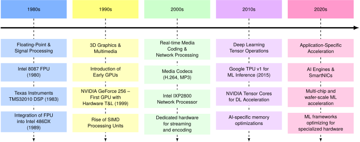
Across five eras from the 1980s to the 2020s (figure 3), specialization moved from discrete coprocessors such as the Intel 8087 FPU and TMS32010 DSP through graphics engines and dedicated media codecs to deep-learning tensor arrays and wafer-scale hardware. Each era’s specialized unit targets a different bottleneck, yet the principles modern accelerators depend on (dedicating silicon to the dominant operation, staging operands in local memory, and minimizing off-chip data movement) were all in place before deep learning arrived.
11.2.2 Domain-specific architectures
A general-purpose CPU core spends most of its energy on instruction fetch and decode, branch prediction, speculative execution, and cache coherence rather than arithmetic: executing one scalar instruction can burn hundreds of picojoules of control overhead just to perform a floating-point operation that costs a few picojoules. For decades, Moore’s law3 (Moore 1998) and Dennard scaling (Dennard et al. 1974) hid that overhead by letting operating voltage fall as transistors shrank, so clock frequencies rose at constant power density. When leakage current halted voltage scaling in the mid-2000s, frequencies stalled against the power wall of Physical Constraints on Deployment, and adding more general-purpose cores ran into Amdahl’s law and dark silicon, the thermal limit under which only a fraction of a chip’s transistors can switch at full speed simultaneously (Esmaeilzadeh et al. 2011). As Hennessy and Patterson (2019) argued in their Turing Lecture, the way past this wall is domain-specific architectures (DSAs),4 hardware that gives up general-purpose control machinery to spend its power budget directly on the operations a target domain performs.
3 Moore’s law: Gordon Moore’s 1965 observation, revised in 1975, that the number of transistors per chip doubles roughly every two years (Moore 1998). It describes density, not performance; performance tracked density only while Dennard scaling held.
Moore, G. E. 1998. “Cramming More Components onto Integrated Circuits.” Proceedings of the IEEE 86 (1): 82–85. https://doi.org/10.1109/jproc.1998.658762.
Dennard, Robert H., Frank H. Gaensslen, Hwa-Nien Yu, Victor L. Rideout, Elias Bassous, and Antoine R. LeBlanc. 1974. “Design of Ion-Implanted MOSFET’s with Very Small Physical Dimensions.” IEEE J. Solid-State Circuits 9 (5): 256–68. https://doi.org/10.1109/jssc.1974.1050511.
Esmaeilzadeh, Hadi, Emily Blem, Renee St. Amant, Karthikeyan Sankaralingam, and Doug Burger. 2011. “Dark Silicon and the End of Multicore Scaling.” Proceedings of the 38th Annual International Symposium on Computer Architecture, 365–76. https://doi.org/10.1145/2000064.2000108.
4 DSA (domain-specific architecture): A DSA that excels at dense matrix multiplication may perform worse than a CPU on irregular workloads such as graph traversal, so its gain on the target domain must justify the software, compiler, and ecosystem cost of a narrower machine (Hennessy and Patterson 2019, 2017).
Hennessy, John L., and David A. Patterson. 2019. “A New Golden Age for Computer Architecture.” Communications of the ACM 62 (2): 48–60. https://doi.org/10.1145/3282307.
Hennessy, John L., and David A. Patterson. 2017. Computer Architecture: A Quantitative Approach. 6th ed. Morgan Kaufmann.
Sullivan, Gary J., Jens-Rainer Ohm, Woo-Jin Han, and Thomas Wiegand. 2012. “Overview of the High Efficiency Video Coding (HEVC) Standard.” IEEE Transactions on Circuits and Systems for Video Technology 22 (12): 1649–68. https://doi.org/10.1109/tcsvt.2012.2221191.
Turakhia, Yatish, Gill Bejerano, and William J. Dally. 2018. “Darwin: A Genomics Co-Processor Provides up to 15,000X Acceleration on Long Read Assembly.” Proceedings of the Twenty-Third International Conference on Architectural Support for Programming Languages and Operating Systems (ASPLOS), 199–213. https://doi.org/10.1145/3173162.3173193.
Bedford Taylor, Michael. 2017. “The Evolution of Bitcoin Hardware.” Computer 50 (9): 58–66. https://doi.org/10.1109/mc.2017.3571056.
A DSA wins by specializing every layer of the machine around the workload’s invariants. Its data path is custom-built; matrix units in AI accelerators are often systolic arrays, grid-like networks of processing elements that compute and forward data directly to neighboring units, so a value fetched once from on-chip memory is reused across an entire row or column of multiply-accumulate operations instead of returning to a register file after each use. Its memory hierarchy follows the workload’s reuse pattern, with software-managed scratchpads and prefetching replacing hardware-managed caches for deterministic tensor streams. Its instruction set encodes coarse tensor operations, so one macro-instruction configures thousands of arithmetic units. The same recipe produced smartphone video codecs, genomics aligners, and cryptographic application-specific integrated circuits (ASICs) wherever a kernel stabilized (Sullivan et al. 2012; Turakhia et al. 2018; Bedford Taylor 2017).
The pressure to specialize has grown because model demand has outrun single-device hardware scaling. The measured trend is the historical training-compute curve charted in Introduction, whose fitted doubling time runs from 3.4 to about 6 months depending on the window, far faster than the roughly two-year doubling of transistor density (Amodei and Hernandez 2018; Epoch AI 2024). No single chip closes a gap that compounds at that rate; parallelism and co-design must close the rest.
Amodei, Dario, and Danny Hernandez. 2018. “AI and Compute.” OpenAI Blog 2.
Epoch AI. 2024. Machine Learning Trends. Epoch AI Research Database.
↩︎ The measured growth of training compute and its doubling time are established in Three Dimensions of ML Efficiency.
11.2.3 Machine learning hardware specialization
When Google projected in 2013 that three minutes of daily voice search per user would require doubling its global CPU fleet just to run neural-network inference (example 11.2), the bottleneck was not a shortage of servers but a mismatch between neural networks and general-purpose cores. Many important neural-network workloads concentrate their work in regular tensor operations, such as dense matrix multiplications and convolutions, with substantial data parallelism, predictable reuse, and tolerance for reduced precision. Other ML operations remain irregular, bandwidth bound, or too small to fill a wide engine, so an accelerator need not speed up every part of a model; hardware built to exploit the regular portion forms the class of ML accelerators.
Example 11.2: The TPU capacity cliff
Scenario: Google projected in 2013 that user adoption of voice-search speech recognition (3 minutes/day/user) would require doubling global data center capacity to run CPU-based neural network inference (Jouppi et al. 2017).
Diagnosis: General-purpose CPU server capacity was economically unable to absorb the exponential growth in inference FLOPs, threatening a capital infrastructure bottleneck.
Systems lesson: Custom hardware acceleration becomes a candidate when workload volume makes the existing fleet uneconomical. Workload reuse, supported operations, development cost, and server total cost of ownership determine whether a custom ASIC is preferable to software changes or other hardware.
A general-purpose CPU is a poor host for this work. Take the chapter’s reference CPU, the low end of the 1–2 TFLOP/s baseline used in the definition of hardware acceleration, and assume it sustains 5 percent–10 percent of its peak on a neural network workload. The upper endpoint then delivers approximately 100 GFLOP/s (billions of floating-point operations per second). CPUs optimize for single-thread performance and irregular memory access, whereas neural networks require massive parallelism and predictable data streams, and a single layer that touches gigabytes of parameters overwhelms cache hierarchies designed for smaller working sets.
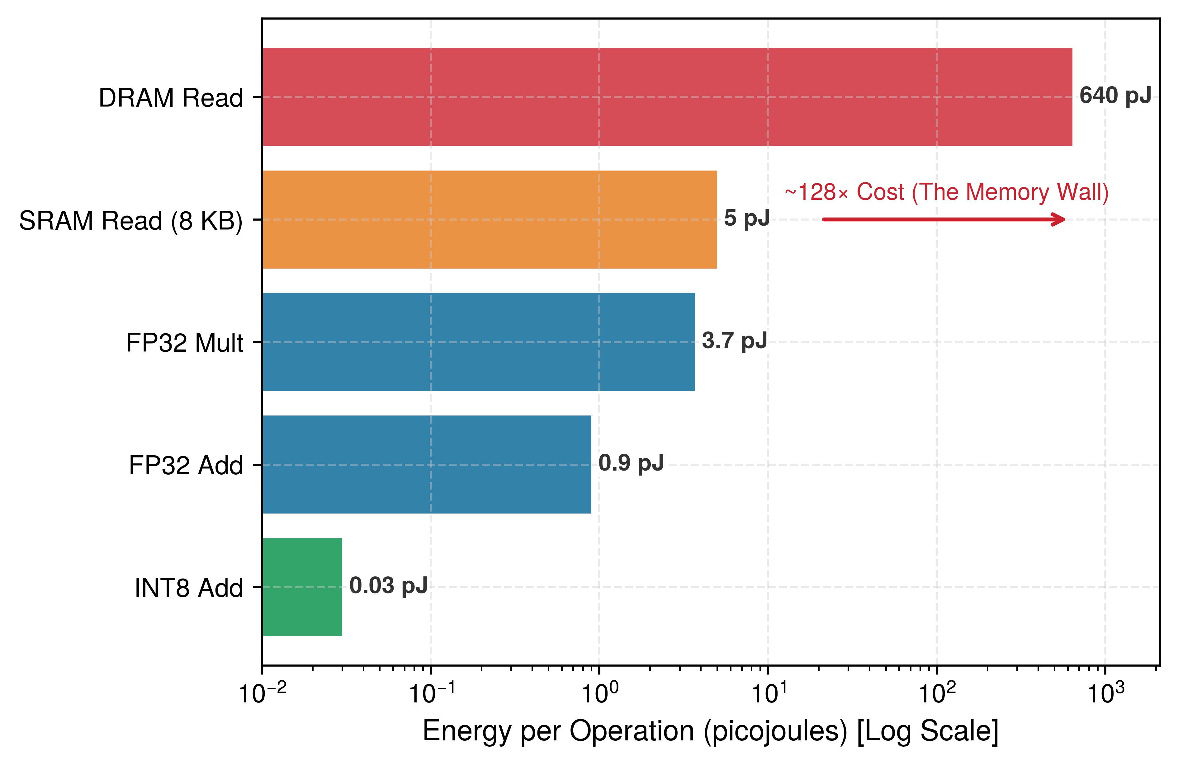
The deeper mismatch is energy. Per event, accessing a 32-bit value from DRAM costs about 640 pJ in the 45 nm estimates of Horowitz (2014), roughly 173× the 3.7 pJ of one FP32 multiply, the same ratio Energy Cost of Moving vs. Computing on a 32-Bit Value reported for the data pipeline. The roughly 145-fold gap quoted with the iron law in Iron Law of ML Systems comes from the same table but compared one DRAM byte, a quarter of this 32-bit access, with one FP16 operation. Exact values vary by technology node and design, but a gap of two orders of magnitude, the energy-movement principle (7), makes data movement a primary optimization target (Sze et al. 2017). Purpose-built accelerators such as TPUs sustain high utilization on dense kernels because systolic arrays and similar structures maximize data reuse while minimizing movement.
5 Von Neumann bottleneck: Separating storage from compute requires instructions and data to cross interfaces rather than remain in local registers. The exact cost of each crossing changes with technology and operation, but locality remains a first-order design concern.
Data access can dominate the energy budget of a memory-intensive kernel.5 On a logarithmic scale, representative 45 nm operation energies span more than four orders of magnitude, from an INT8 addition (\(0.03\text{ pJ}\)) and an FP32 multiply (\(3.7\text{ pJ}\)) to an off-chip DRAM fetch (\(640\text{ pJ}\)) (figure 4). This ladder is the chapter’s single reference for what moving a value costs; later sections cite it rather than restate it.
Training and inference load an accelerator differently. Training computes gradients, typically in mixed precision with lower-precision tensor operations and higher-precision accumulation (Micikevicius et al. 2018), and backpropagation retains or recomputes activations, raising memory demand. Inference requires only the forward path and may use INT8 or INT4 when the model and kernels support it. The service objective, whether tail latency, throughput, cost, or energy, then decides which accelerator fits.
↩︎ The activation memory that backpropagation must retain is established in Activation memory requirements.
Definition 11.3: ML accelerator
Machine Learning Accelerators are processors or specialized units designed primarily for common neural-network tensor operations and dataflows. They pursue high \(\PeakRate\) and data reuse on matching workloads by devoting more resources to arithmetic and local data movement than a general-purpose execution path can.
- Significance: An ML accelerator’s defining feature is not raw arithmetic alone but a balanced path that supplies operands and retains reusable values nearby. The H100 provides 3.35 TB/s of device-memory bandwidth, about 16.8× the illustrative 200 GB/s host-DRAM path used here (Choquette 2023). This is a ceiling comparison, not a guarantee: sufficient arithmetic intensity, concurrency, and reuse are still required to approach its 989 TFLOP/s dense FP16/BF16 peak.
- Distinction: The gains are conditional on operation support, parallel work, regular data access, and a software stack that selects the intended path. An ML accelerator can be orders of magnitude faster than a reference CPU on large dense matrix multiplication, yet lose much of that advantage on small, irregular, synchronization-heavy, or control-heavy workloads. Transfers and unsupported operators can dominate even when the accelerated kernel itself is fast.
- Common pitfall: A frequent misconception is that ML accelerators always accelerate ML. Approaching peak throughput requires a compatible precision, operation shape, layout, and enough parallel work to keep the relevant units busy, and memory and interconnect paths must sustain that work. A batch-1 autoregressive request may therefore use only a small fraction of a large training accelerator’s arithmetic capacity even though the same device performs well on batched prefill or training.
Deployment context decides which constraint binds. In data centers it is often time-to-result for training large models. An NVIDIA H100 trades hundreds of watts of power for high throughput (Choquette 2023), and Google’s TPUv4 makes a similar trade through systolic arrays and high-bandwidth memory (Jouppi et al. 2023); whether either lowers total cost depends on utilization, rental price, workload scaling, and the electricity rate.
At the edge, the priority shifts toward energy per inference and hard latency or power limits. A smartphone camera or always-on audio path inside a few-watt budget cannot adopt a data center memory system, so edge architectures reduce movement through local scratchpads, tight integration, and dynamic voltage and frequency scaling. Because the binding constraint differs by setting, no single architecture dominates, yet the memory wall governs both. Data center chips buy capacity and bandwidth with HBM, while edge chips depend on proximity and reuse.
Checkpoint 11.2: The accelerator gate
The energy hierarchy decides when specialization pays.
Energy hierarchy
Selection logic
11.2.4 The integration bottleneck
Packing thousands of multiply-accumulate units onto a die buys nothing if those units spend most cycles stalled waiting for operands to cross the memory hierarchy. From the 8087 onward, hardware has evolved to fit the algorithm’s dominant bottleneck (Palmer 1980; Sze et al. 2017; Jouppi et al. 2017), and for dense matrix multiplications and convolutions the remaining difficulty is feeding the arithmetic units. The integration bottleneck is the memory wall seen from inside the accelerator: transporting operands and results through the memory hierarchy quickly and efficiently enough to keep thousands of parallel compute units busy. Specialized silicon delivers its performance-per-watt advantage only when the workload’s demand concentrates into regular operations that align with the hardware’s data paths.
6 Scratchpad memory: When a compiler can determine a tensor kernel’s access pattern, it can explicitly stage tiles in fast, software-controlled local memory. This avoids some tag, replacement, and coherence machinery, but transfers, synchronization, banking, and capacity must be scheduled correctly. Scratchpads complement rather than universally replace caches because irregular or shared data may still benefit from hardware management. Google’s TPU v1, for example, used a 24 MB software-managed Unified Buffer for intermediate activations, while weights and instructions used other paths (Jouppi et al. 2017).
Jouppi, Norman P., Cliff Young, Nishant Patil, David Patterson, Gaurav Agrawal, Raminder Bajwa, Sarah Bates, et al. 2017. “In-Datacenter Performance Analysis of a Tensor Processing Unit.” Proceedings of the 44th Annual International Symposium on Computer Architecture, ISCA ’17, 1–12. https://doi.org/10.1145/3079856.3080246.
Neural-network kernels make this integration bottleneck tractable because their arithmetic, dataflow, and numerical requirements reinforce one another. Large matrix multiplications and convolutions expose abundant data parallelism that dense processing-element arrays can execute concurrently, and because static or compiled tensor graphs move those operands along predictable paths, compilers can tile and stage transfers into local scratchpads6 instead of relying exclusively on hardware-managed caches. Those staged operands also tolerate reduced precision, allowing supported 8-bit or 4-bit paths to pack more values into each scratchpad and multiply them more densely (Dally et al. 2021; Dally 2023). Workloads dominated by dynamic control flow, large embedding tables, small tensors, variable shapes, or strict precision requirements break these assumptions and remain bound by memory latency and irregular access.
Once arithmetic capacity is abundant, the central engineering challenge shifts to staging data close to compute. Given the 173× energy penalty of off-chip DRAM transfers, accelerator architects deliberately allocate silicon area and thermal budgets to stacked HBM, wide on-chip SRAM, and software-managed scratchpads rather than packing in additional floating-point logic.7 Those are the memory tiers drawn in figure 1, and they occupy as much of the design as the arithmetic units they feed.
7 HBM: The A100 and H100 generations provide 2.0–3.4 TB/s of device-memory bandwidth through stacked memory and wide interfaces, compared with 760 GB/s for the GDDR6X reference used here (NVIDIA Corporation 2020a; Choquette 2023). Raising the bandwidth ceiling can move some kernels toward the compute-bound side of the roofline, but only if their access pattern and arithmetic intensity can use it. HBM also increases packaging and system cost, so its value depends on the workload’s bandwidth demand.
The specialization evident in processing elements, vector pipelines, and tiered scratchpads reflects the computational profile of neural networks, which repeatedly invoke a compact set of linear-algebraic and element-wise primitives. Within the D·A·M framework, an algorithmic change produces a wall-clock speedup only when its computational structure and memory access pattern map onto these primitives; one that cuts theoretical operations without aligning with the hardware’s data paths leaves compute units starved. The next section identifies those primitives, beginning with the multiply-accumulate that carries nearly all of ResNet-50’s arithmetic.
Self-Check: Question
What primary physical limitation brought about the end of Dennard scaling in the mid-2000s, necessitating the transition from increasing CPU clock frequencies to domain-specific hardware accelerators?
- Lithography light diffraction preventing further reduction of transistor gate length below \(1\,\mu\text{m}\)
- Inability to lower operating voltage proportionally with transistor size, leading to unsustainable power density and heat dissipation limits
- Quantum tunneling in copper interconnect lines preventing data transmission between arithmetic units
- Depletion of global silicon substrate supplies requiring migration to gallium nitride semiconductors
Contrast the architectural trade-offs of software-managed scratchpad memory (such as Google TPUv1’s Unified Buffer) with hardware-managed cache hierarchies when executing large-scale tensor workloads.
Place the following computing milestones in chronological order (from earliest to most recent) as hardware evolved toward modern AI accelerators:
- Introduction of dedicated Tensor Cores and TPUs for deep learning matrix operations
- Emergence of fixed-function media codecs and network processors for video/packet streaming
- Integration of floating-point units (FPUs) and digital signal processors (DSPs) as discrete coprocessors
- General-purpose programmable GPUs and SIMD instruction set extensions for 3D graphics and multimedia
True or False: Google’s TPUv1 achieved substantial performance-per-watt improvements over contemporary general-purpose CPUs primarily by operating at significantly higher clock frequencies.
Why has the pressure to build specialized ML hardware grown since the 2012 deep learning breakthrough?
- Consumer mobile SoCs began to exceed data center GPUs in memory bandwidth
- On-chip SRAM latency rose relative to host DRAM latency over PCIe
- Training compute demand has doubled every few months while transistor density doubles roughly every two years, so no single chip can keep pace without parallelism and co-design
- Python framework dispatch overhead grew faster than GPU kernel execution time
11.3 Compute Primitives
A single forward pass through a neural network layer can issue millions or billions of MAC operations, and executing them one scalar instruction at a time would swamp the processor in instruction-fetch and register-access overhead. Across fully connected, convolutional, and attention layers, learned linear transformations reduce to these repeated MACs, whose regular tensor structure exposes the parallel work and operand reuse that hardware specialization requires. MACs do not dominate every model or phase (normalization, routing, indexing, communication, and element-wise operations can become limiting), but they account for much of the peak arithmetic capacity in modern ML accelerators. Whether they dominate elapsed time still depends on tensor shape, data movement, and the surrounding operators.
The hardware units that exploit these patterns are AI compute primitives: specialized functional blocks, each optimized for a particular class of operation. Three primitives are especially common in accelerators, each targeting a distinct computational pattern found in neural networks; at the framework level, a single declarative statement encapsulates thousands of their arithmetic operations (listing 1).
# Framework abstracts compute-intensive operations
dense = Dense(512)(input_tensor)  # 256x512 MACs per sample
Beneath this API call, an autograd or compilation engine lowers the layer into a computational graph. Listing 2 exposes a bulk matrix multiplication and bias broadcast, followed by an optional element-wise activation; the activation is a separate stage rather than an implicit part of the shown Dense call.
# Linear transformation work scales with input_dim x output_dim x
# batch.
output = (
    matmul(input, weights) + bias
)  # Matrix multiply dominates cost
output = activation(
    output
)  # Element-wise: proportional to output_dim x batch
While graph representations group these steps into coarse tensor operators, execution on physical hardware requires scheduling individual scalar operations. Lowering the matrix multiplication to loop nests (listing 3) makes the execution structure explicit: three nested iterations traverse the batch, output feature, and reduction dimensions, establishing \(\mathcal{O}(\BatchSize\times \LayerInputWidth \times \LayerOutputWidth)\) arithmetic complexity.
# Total operations: batch_size × output_size × input_size MACs
for n in range(batch_size):  # Batch dimension: parallelizable
    for m in range(output_size):  # Output neurons: parallelizable
        sum = bias[m]  # Initialize accumulator
        for k in range(input_size):  # Reduction dimension: sequential
            sum += input[n, k] * weights[k, m]  # MAC operation
        output[n, m] = activation(sum)  # Nonlinear transformation
# Example work scales as batch_size × output_size ×
# input_size multiply-accumulate operations
These nested loops expose three recurring computational patterns: element-wise operations along vectors, matrix-level multiply-accumulate reductions, and nonlinear transformations. Their ubiquity justifies dedicated hardware execution paths: vector pipelines stream independent elements and reductions, matrix engines organize multiply-accumulate grids across spatial tiles, and special-function units approximate nonlinear math. The boundaries between these units are architectural rather than mathematical; an optimizing compiler frequently fuses operations across all three paths within a single kernel invocation to eliminate intermediate memory traffic.
11.3.1 Vector operations
In the scalar loop nest of listing 3, evaluating a batch of 32 samples through a 256-to-512 dense layer requires 4.2M MACs, and a scalar processor must fetch and decode separate instructions to load each input-weight pair, multiply-accumulate them, and advance the loop counters. Vector architectures eliminate this per-element control overhead by packing multiple data elements into wide register files (typically 128 to 512 bits) and applying a single decoded instruction across parallel execution lanes simultaneously.
RISC-V,8 an open instruction-set architecture (ISA) with a standardized vector extension (Waterman et al. 2013), provides a concrete vehicle for this execution model. The contiguous loads in listing 4 assume that the selected weight column has been packed into a contiguous vector; the row-major weights[k, m] access in the scalar example is otherwise strided. In RISC-V vector assembly, code is decoupled from fixed hardware widths: the instruction vsetvli queries the hardware to determine how many elements fit into available registers, processes that chunk, and loops until all features are exhausted.
8 RISC-V (reduced instruction set computer V): The open ISA allows hardware teams to add custom ML instructions, including vector dot products, activation functions, and sparse tensor operations, without changing the base ISA. The trade-off is software ecosystem maturity: custom extensions require corresponding compiler, library, and runtime support, which can limit portability and increase integration work.
Waterman, Andrew, Yunsup Lee, Rimas Avizienis, Henry Cook, David Patterson, and Krste Asanovic. 2013. “The RISC-V Instruction Set.” 2013 IEEE Hot Chips 25 Symposium (HCS), 1–1. https://doi.org/10.1109/hotchips.2013.7478332.
fmv.w.x fa0, zero          # Scalar dot-product accumulator
fmv.w.x ft1, zero          # Zero seed for vector reduction
loop_feature:
    vsetvli t0, feature_cnt, e32, m1, ta, ma
    vle32.v v1, (in_ptr)
    vle32.v v2, (wt_ptr)
    vfmul.vv v3, v1, v2
    vfmv.v.f v0, ft1
    vfredusum.vs v4, v3, v0
    vfmv.f.s ft0, v4
    fadd.s fa0, fa0, ft0
    slli t1, t0, 2         # Four bytes per FP32 element
    add in_ptr, in_ptr, t1
    add wt_ptr, wt_ptr, t1
    sub feature_cnt, feature_cnt, t0
    bnez feature_cnt, loop_feature
Each pass of the loop in listing 4 asks the hardware how many 32-bit elements fit in its vector registers (vsetvli), loads that many input and weight elements with two wide loads (vle32.v), multiplies them lane by lane (vfmul.vv), reduces the products into a partial sum (vfredusum.vs), and advances the pointers until no elements remain. One decoded instruction thus does the work of a whole chunk of scalar instructions.
Across iterations, the vector multiply instruction processes multiple data elements concurrently while wide loads amortize instruction decode and memory-request overhead. Because the runtime vector length dynamically adapts to the implementation’s hardware width (VLEN), the identical binary executes correctly on both narrow embedded vector units and wide data-center pipelines. For this 256-feature workload, an 8-lane implementation breaks the reduction into approximately 524,288 vector chunks across the batch.
Beyond dense inner products, deep learning workloads rely on a broader set of vector instructions. Table 2 maps these primitive vector operations to the specific neural network layers that depend on them.
| Vector operation | Description | Neural network application |
|---|---|---|
| Reduction | Combines elements across a vector (for example, sum, max) | Pooling layers, attention score computation |
| Gather | Loads multiple nonconsecutive memory elements | Embedding lookups, sparse operations |
| Scatter | Writes to multiple nonconsecutive memory locations | Gradient updates for embeddings |
| Masked operations | Selectively operates on vector elements | Attention masks, padding handling |
| Vector-scalar broadcast | Applies scalar to all vector elements | Bias addition, scaling operations |
The benefit extends beyond instruction count. Contiguous vector loads can use memory interfaces efficiently, and control overhead is amortized across several data elements. Gather, scatter, masking, and short tails may use fewer lanes or require extra memory transactions, so vector width alone does not guarantee proportional speedup. The architectural pattern is not new. The Cray-19 used vector registers and pipelined functional units for scientific computing in the 1970s (Jordan 1982); modern ML processors apply related principles at much larger commercial scale. In ResNet-50 the vector path carries the ReLU after every convolution and the residual addition that closes every bottleneck block. Each touches every activation element once and performs about one operation per element, so on its own it is limited by how fast the activations stream past, not by lane count.
9 Cray-1 vector legacy: The Cray-1 (1975) used 64-element vector registers with pipelined functional units, allowing a stream of elements to advance through arithmetic operations without issuing one scalar instruction per element. Modern accelerators extend the same principles of wide registers, pipelined execution, and data reuse to vector and matrix tiles.
Jordan, T. L. 1982. “A Guide to Parallel Computation and Some Cray-1 Experiences.” In Parallel Computations. Elsevier. https://doi.org/10.1016/b978-0-12-592101-5.50006-3.
Vector operations excel at element-wise transformations such as activation functions, where each output depends only on its corresponding input. Neural networks, however, also require structured computations where each output depends on all inputs, the weighted sums that define layer transformations. These many-to-many operations naturally express themselves as matrix multiplications, the second compute primitive.
11.3.2 Matrix operations
Evaluating a dense layer one vector dot product at a time wastes reuse: each weight row is loaded for one sample and discarded before the next sample in the batch arrives, and each input vector is re-read for every output neuron. Matrix multiplication eliminates this redundant traffic by organizing work across two-dimensional tiles of weights, activations, and gradients, accounting for much of the arithmetic in dense neural networks (Goodfellow et al. 2016). Hardware and libraries tile those dimensions so blocks of weights and activations are reused across an entire tile while partial sums accumulate locally, though small or irregular matrices can still leave tile capacity unused.
Matrix operations in neural networks
Neural network computations decompose into hierarchical matrix operations. Listing 5 captures this hierarchy through a linear layer that transforms input features into output neurons over a batch. Its expanded mathematics uses a column-batch convention and adds an optional ReLU; this illustrates the arithmetic rather than the framework API’s internal tensor layout or an activation implicit in nn.Linear.
layer = nn.Linear(256, 512)  # Layer transforms 256 inputs to 512 outputs
output = layer(input_batch)  # Process a batch of 32 samples

# Framework Internal: Core operations (column-batch convention)
Z = matmul(weights, input)  # Matrix: transforms [256×32]
# input to [512×32] output
Z = Z + bias  # Vector: adds bias to each
# output independently
output = relu(Z)  # Vector: applies activation to
# each element independently
The scale of this matrix work follows from the layer dimensions. Each output neuron (512 total) must process all input features (256 total) for every sample in the batch (32 samples). The weight matrix alone contains 256 \(\times\) 512 = 131,072 parameters that define these transformations, illustrating why efficient matrix multiplication dominates performance considerations.
Neural networks employ matrix operations across architectural patterns beyond simple linear layers. Convolution operations transform into matrix multiplications through the im2col technique,10 enabling efficient execution on matrix-optimized hardware. Listing 6 illustrates these applications.
10 Im2col (image-to-column): The im2col lowering of Computational mapping turns convolution into a matrix multiplication by unfolding each receptive-field patch into one row or column of a dense matrix. An explicit materialization can duplicate overlapping values and expand storage by up to roughly the kernel area before edge, stride, and channel effects are considered. Production libraries often use implicit-GEMM or direct-convolution kernels to obtain matrix-friendly execution without materializing the full expanded matrix.
hidden = matmul(weights, inputs)
# weights: [out_dim x in_dim], inputs: [in_dim x tokens]
# Result combines all inputs for each output

# Attention Mechanisms - Multiple matrix operations
Q = matmul(Wq, inputs)
# Project inputs to query space [query_dim x tokens]
K = matmul(Wk, inputs)
# Project inputs to key space [key_dim x tokens]
attention = matmul(Q.T, K)
# Compare all query tokens with all key tokens [tokens x tokens]

# Convolutions - Matrix multiply after reshaping
patches = im2col(input)
# Convert [H x W x C] image to matrix of patches
output = matmul(kernel, patches)
# Apply kernels to all patches simultaneously
These examples differ in tensor shape and reuse pattern, which determines how efficiently each multiplication occupies a matrix unit. Linear layers reuse one weight matrix across a batch; attention forms projections and then a token-to-token score matrix; convolution reuses each kernel across many image patches. Expressing all three as matrix multiplication exposes a common interface to hardware, but it does not make their execution costs identical. Batch size, sequence length, channel count, and tiling determine whether operands are reused locally or repeatedly fetched from memory. For ResNet-50 the lowering is nearly total: every convolution and the final fully connected layer become matrix multiplications, so almost all of its operations run on whatever matrix hardware the accelerator provides, and the INT8 profile of Model Compression is in effect a statement about that hardware.
Matrix operations hardware acceleration
Accelerators therefore need units that handle whole tiles. Listing 7 demonstrates a representative dedicated matrix unit that processes an entire \(16{\times}16\) block at once, illustrating why matrix instructions and Tensor Cores can deliver much higher throughput than scalar or vector-only execution paths (NVIDIA 2017; Intel Corporation 2021a).
mload mr1, (weight_ptr)     # Load e.g., 16x16 block of
                            # weight matrix
mload mr2, (input_ptr)      # Load corresponding input block
matmul.mm mr3, mr1, mr2     # Multiply and accumulate entire
                            # blocks at once
mstore (output_ptr), mr3    # Store computed output block
The illustrative unit operates on matrix tiles rather than individual elements. A full \(16{\times}16{\times}16\) tile product contains \(16^3=4{,}096\) multiply-accumulate operations, but the cycles required depend on the actual instruction and architecture. Sustained throughput also depends on the number of matrix units, operand precision, issue rate, pipeline behavior, and whether memory can keep the units fed. Matrix units complement vector execution by accelerating structured many-to-many transformations.
Much like vector processing, matrix acceleration has deep historical roots; digital signal processors (DSPs) and graphics processors optimized matrix computations in the 1980s–1990s for image processing, scientific computing, and 3D rendering (Owens et al. 2008; Hwu 2011). Neural networks have made matrix multiplication commercially dominant, driving the integration of two-dimensional systolic arrays and matrix execution engines (such as NVIDIA Tensor Cores and Google TPUs) directly into processor datapaths.
Owens, John D., Mike Houston, David Luebke, Simon Green, John E. Stone, and James C. Phillips. 2008. “GPU Computing.” Proceedings of the IEEE 96 (5): 879–99. https://doi.org/10.1109/jproc.2008.917757.
Hwu, Wen-mei W. 2011. “Introduction.” In GPU Computing Gems Emerald Edition. Elsevier. https://doi.org/10.1016/b978-0-12-384988-5.00064-4.
Linear algebra constitutes only part of the neural network execution pipeline. Between linear transformations, neural networks introduce nonlinear activation functions and normalization layers. While piecewise-linear functions such as ReLU map to simple vector comparison instructions, transcendental computations (such as exponentials in softmax and GELU, or reciprocal square roots in normalization) cannot be computed directly on multiply-accumulate datapaths without incurring severe cycle penalties. Table 3 summarizes the execution characteristics of the three primary compute primitives and their mapping to neural network operations.
| Operation type | Best For | Examples | Key characteristic |
|---|---|---|---|
| Matrix Operations | Many-to-many transforms | Layer transformations, attention, convolutions | Each output depends on multiple inputs |
| Vector Operations | Vector and reduction work | Activation functions, layer normalization, element-wise gradients | Uses element-wise operations and vector reductions |
| Special-Function Paths | Transcendental arithmetic | Exponential, logarithm, reciprocal square root | Uses architecture-specific approximation or dedicated logic |
11.3.3 Special function units
Evaluating an exponential in softmax, a hyperbolic tangent in GELU, or a reciprocal square root in layer normalization on standard multiply-accumulate hardware requires a multi-instruction polynomial approximation that can stall the pipeline between fast matrix kernels. Special Function Units (SFUs) and specialized instruction paths remove this bottleneck, completing the chapter’s trio of processing primitives. The need is not new: floating-point coprocessors addressed scalar arithmetic bottlenecks (Palmer 1980), and digital signal processors added specialized arithmetic for signal-processing workloads (Smith 1997). An implementation may use a standalone unit, vector approximation instructions, or a library sequence, trading accuracy, latency, and throughput. In neural networks, activation, normalization, and softmax operations can become the limiting stage between matrix kernels when repeated memory passes or transcendental functions cap throughput.
Palmer, John F. 1980. “The Intel 8087 Numeric Data Processor.” Proceedings of the 1980 National Computer Conference (AFIPS), 887–93. https://doi.org/10.1145/1500518.1500674.
Smith, Steven W. 1997. “Digital Signal Processing.” In Digital Signal Processing Demystified. Elsevier. https://doi.org/10.1016/b978-187870716-1/50004-4.
Nonlinear functions
A common layer sequence illustrates how non-matrix operators enter the execution pipeline (Goodfellow et al. 2016). Listing 8 chains a linear transformation with ReLU activation and batch normalization, operations that appear trivial in Python framework code but impose distinct arithmetic and memory constraints on hardware.
Goodfellow, Ian, Yoshua Bengio, and Aaron Courville. 2016. Deep Learning. MIT Press.
layer = nn.Sequential(
    nn.Linear(256, 512), nn.ReLU(), nn.BatchNorm1d(512)
)
output = layer(input_tensor)
Listing 9 expands this sequence into its arithmetic primitives, isolating the element-wise thresholding of ReLU from the cross-batch reductions and reciprocal square root required by batch normalization. Here rows are samples and columns are features; weights has input features by output features, while bias, gamma, and beta contain one value per output feature. Keeping the reduced batch dimension permits those per-feature statistics to broadcast across samples.
Z = matmul(input, weights) + bias  # Linear transformation
H = max(0, Z)  # ReLU activation
mean = reduce_mean(H, axis=0, keepdims=True)  # BatchNorm statistics
var = reduce_mean((H - mean) ** 2, axis=0, keepdims=True)  # Variance computation
output = gamma * (H - mean) / sqrt(var + eps) + beta  # Normalization
Hardware implementation of nonlinear functions
Translating these mathematical functions to silicon exposes sharp differences in memory traffic, instruction count, and pipeline utilization. For instance, batch normalization (Ioffe and Szegedy 2015) demands multi-pass statistics gathering across memory, variance accumulation, and a reciprocal square root, while softmax requires computing exponentials across an entire normalization dimension. While a rectified linear unit (ReLU) is mathematically simple, a naive scalar implementation incurs branch overhead or redundant memory round-trips unless fused into adjacent kernels. Listing 10 contrasts the memory and dependency overheads of pointwise activation against multi-pass normalization in an unfused loop model.
Ioffe, Sergey, and Christian Szegedy. 2015. “Batch Normalization: Accelerating Deep Network Training by Reducing Internal Covariate Shift.” Proceedings of the 32nd International Conference on Machine Learning (ICML) 37: 448–56.
The label nonlinear hides three different execution patterns. Pointwise functions such as ReLU leave elements independent and therefore map naturally to vector lanes or parallel threads. Reductions such as the mean and variance in batch normalization introduce cross-element dependencies: partial results must be combined before later stages can proceed. Transcendental functions such as exponential, logarithm, and reciprocal square root add a numerical trade-off because their implementations balance latency, precision, and valid input range. The dependency pattern, not the mathematical label alone, determines whether vector arithmetic, a reduction tree, or a specialized approximation path is appropriate. A faster special-function path accelerates only the operation it implements; it does not remove surrounding tensor traffic or synchronization.
Listing 10 is intentionally dependency-explicit rather than a model of an optimized kernel. The loops expose three state lifetimes: per-element activations, per-feature accumulators, and the final normalized outputs. The normalization parameters cannot be applied until the required statistics are available, so implementations must either retain intermediate activations or recompute them. Training derives those statistics from the current batch, whereas inference can use stored statistics and reduce normalization to an element-wise affine transform. Compilers may fuse legal stages, but the data dependencies determine which transformations preserve the computation. Reading the listing as a dependency graph therefore reveals the durable hardware questions: how often each tensor crosses a memory interface, which intermediates remain local, and where reductions impose synchronization.
for batch in range(32):
    for feature in range(512):
        # ReLU: Naive scalar compare/select; optimized kernels
        # usually implement this branchlessly.
        z = matmul_output[batch, feature]
        h = max(0.0, z)  # Conditional operation

        # BatchNorm: Multiple passes over data
        mean_sum[feature] += h  # First pass for mean
        var_sum[feature] += h * h  # Additional pass for variance

        temp[batch, feature] = h  # Extra memory storage needed

# Normalization requires complex arithmetic
for feature in range(512):
    mean = mean_sum[feature] / batch_size
    var = (var_sum[feature] / batch_size) - mean * mean

    # Square root computation: Multiple iterations
    scale = gamma[feature] / sqrt(var + eps)  # Iterative
    # approximation
    shift = beta[feature] - mean * scale

    # Additional pass over data for final computation
    for batch in range(32):
        output[batch, feature] = temp[batch, feature] * scale + shift
The dependency structure in listing 10 exposes two costs of naive execution. The pointwise ReLU and normalization scale-and-shift perform little arithmetic per accessed byte, so materializing each pass can place a low bandwidth ceiling on throughput. In this unfused loop model, temp is stored and reread after batch statistics are finalized; its physical traffic depends on cache residency and the chosen memory interface. Computing \(1/\sqrt{\text{var} + \NumericalStabilityConstant}\) also adds a dependent arithmetic path. The listing illustrates an iterative approximation, but actual kernels may use a reciprocal-square-root instruction and refinement, with device- and accuracy-dependent latency. Specialized function paths address this arithmetic cost, while legal fusion and local buffering reduce intermediate traffic. Neither removes the need to complete the reductions before normalization.
SFU hardware implementation
SFUs address arithmetic bottlenecks by implementing nonlinear and transcendental operations in specialized functional units rather than multi-instruction software routines. Accelerators deploy dedicated datapath circuits, such as quadratic polynomial interpolators and small lookup tables (LUTs), that evaluate functions like exponential, reciprocal square root, and logarithm within a few pipeline stages. Listing 11 illustrates how an instruction set exposes these operations alongside vector memory accesses.
vld.v v1, (input_ptr)    # Load vector of values (pseudocode)
vrelu.v v2, v1           # Vector ReLU path
vsigm.v v3, v1           # Vector sigmoid path
vtanh.v v4, v1           # Vector tanh path
vrsqrt.v v5, v1          # Vector reciprocal-square-root path
Specialized function paths balance circuit area against mathematical precision. While piecewise linear activations such as ReLU require only single-cycle compare-and-select (maximum) datapath logic, transcendental functions trade off lookup table size and polynomial interpolation degrees against approximation error. Representative mechanisms and their qualitative latencies differ by function (table 4).
| Function unit | Operation | Implementation strategy | Illustrative latency |
|---|---|---|---|
| Activation unit | ReLU | Compare-and-select or maximum | Low; architecture-dependent |
| Statistics unit | Mean, variance | Parallel reduction trees | Grows with reduction depth |
| Exponential unit | exp, log, sigmoid, tanh | Approximation, table lookup, and interpolation | Architecture-dependent |
| Root/power unit | sqrt, rsqrt | Iterative or approximation hardware | Architecture-dependent |
The two lighthouses use this path very differently. ResNet-50 barely touches it: its only activation is ReLU, a comparison, and its only exponentials are the thousand in its final softmax. GPT-2 XL leans on it at every step, because each attention head applies softmax across the whole context and each feed-forward block applies GELU, so its special-function work grows with sequence length while ResNet-50’s stays fixed.
Vector operations, matrix operations, and special-function paths establish the foundational arithmetic primitives of ML accelerators, but functional units alone do not dictate sustained throughput. These primitives govern what the silicon computes; the execution model and memory hierarchy govern how data feeds the datapath. A matrix unit rated for hundreds of teraFLOP/s will idle if memory bandwidth cannot sustain operand delivery, if tile dimensions mismatch register blocking, or if thread synchronization serializes execution. Peak assumes operands are always ready; the execution model decides how much of it a real workload achieves.
Self-Check: Question
When executing a Transformer layer containing attention projection (\(Q = X W_q\)), Softmax (\(\text{Softmax}(S)\)), Layer Normalization (\(\text{LayerNorm}(X)\)), and GeLU activation (\(\text{GeLU}(Z)\)), which execution unit is specifically responsible for computing transcendental functions (exponential and error function approximations)?
- Systolic 2D Matrix Multiply Units
- Dense Tensor Cores
- Vector Load-Store Memory Controllers
- Special Function Units (SFUs)
Explain how the \(\text{im2col}\) (image-to-column) transformation allows standard 2D convolution operations to execute on high-throughput matrix multiplication hardware (GEMM engines), and describe the primary memory overhead associated with this approach.
True or False: In modern AI accelerators, element-wise vector operations such as residual additions (\(Y = X_1 + X_2\)) achieve higher arithmetic intensity than large matrix-matrix multiplications (\(C = A \cdot B\)).
The hardware transformation technique that enables convolutional layers to execute as matrix multiplications without physically duplicating overlapping patch data in memory is known as ____ GEMM.
Which of the following operations in a modern deep learning architecture exhibits the highest operational arithmetic reuse, making it most suitable for dense 2D systolic arrays and Tensor Cores?
- Batched linear layer matrix multiplication (\(Y = X W\))
- Element-wise ReLU activation (\(\max(0, x)\))
- Channel-wise Batch Normalization mean computation
- Token-wise embedding table lookup
11.4 Compute Units
Applying ReLU to a 512-element vector shows why execution models matter: the operation is simple, but throughput depends on whether the hardware treats those 512 comparisons as scalar instructions, as lanes of a single instruction, multiple data (SIMD) unit, as GPU threads, or as tensor-program fragments. Modern AI processors package the three compute primitives into distinct execution units (vector units for vector work, matrix units such as Tensor Cores and systolic arrays for matrix work, and special function units for nonlinear functions) and then group those units into processing elements. That organization defines how computations are structured and exposed to programmers, and it explains why theoretical capability and delivered throughput diverge.
The packaging follows reuse per operand. For the reference low-precision operations, reading an operand from a register file and moving it across on-chip wires can cost more energy than the arithmetic itself, so each primitive goes to the unit whose dataflow supplies the reuse it offers. In D·A·M terms, this partition binds algorithmic primitives to machine execution paths. Routing dense matrix multiplications through vector pipelines saturates register-file read ports and collapses throughput to a small fraction of peak, while routing low-intensity elementwise work through matrix arrays leaves their lanes idle.
11.4.1 From SIMD lanes to SIMT threads
Even a wide CPU vector unit stalls when streaming through gigabytes of tensor data: cache misses freeze the pipeline for hundreds of cycles waiting on main memory, the instruction reorder buffer fills, and the SIMD lanes sit empty. The vector path of section 11.3.1 follows Flynn’s SIMD execution model, which amortizes instruction fetch and decode by issuing a single decoded instruction across multiple data elements packed into wide vector registers (Flynn 1966). A 512-bit SIMD register processes sixteen 32-bit floating-point values per instruction—an idea carried into fixed-width CPU vector extensions, Arm’s length-agnostic Scalable Vector Extension (SVE) (Stephens et al. 2017), and two-dimensional tile extensions such as Intel’s Advanced Matrix Extensions (AMX) (Intel Corporation 2021a)—but those wide registers still live inside a CPU core built around branch predictors, out-of-order execution logic, and deep cache hierarchies for a few sequential threads. Conditional branching within a vector also requires evaluating divergent paths under bitmasks, further cutting useful lane utilization.
Flynn, M. J. 1966. “Very High-Speed Computing Systems.” Proceedings of the IEEE 54 (12): 1901–9. https://doi.org/10.1109/proc.1966.5273.
Stephens, Nigel, Stuart Biles, Matthias Boettcher, Jacob Eapen, Mbou Eyole, Giacomo Gabrielli, Matt Horsnell, et al. 2017. “The ARM Scalable Vector Extension.” IEEE Micro 37 (2): 26–39. https://doi.org/10.1109/mm.2017.35.
Lindholm, Erik, John Nickolls, Stuart Oberman, and John Montrym. 2008. “NVIDIA Tesla: A Unified Graphics and Computing Architecture.” IEEE Micro 28 (2): 39–55. https://doi.org/10.1109/mm.2008.31.
Nickolls, John, Ian Buck, Michael Garland, and Kevin Skadron. 2008. “Scalable Parallel Programming with CUDA: Is CUDA the Parallel Programming Model That Application Developers Have Been Waiting For?” Queue 6 (2): 40–53. https://doi.org/10.1145/1365490.1365500.
11 SM (streaming multiprocessor): The physical hardware engine that implements the SIMT model by using warp schedulers to coordinate many parallel threads. Maintaining enough active warps can help hide instruction and memory latency, but occupancy alone does not identify the bottleneck. Low occupancy may result from register use, shared-memory use, block dimensions, or insufficient parallel work, while a memory-bound kernel can still have high occupancy.
Architectures built on single instruction, multiple threads (SIMT) execution resolve these bottlenecks by decoupling the logical programming abstraction from physical hardware execution (Lindholm et al. 2008; Nickolls et al. 2008). Instead of requiring the programmer to pack data into explicit vector registers, SIMT exposes an execution model of independent scalar threads. In GPU architectures, each Streaming Multiprocessor (SM)11 coordinates thousands of concurrent threads. Hardware warp schedulers group these threads into warps, the 32-thread scheduling groups (wavefronts in AMD architectures) whose granularity already set lane utilization in training kernels, and every thread in a warp executes a common instruction in lockstep across parallel ALUs. This lockstep execution introduces a critical constraint known as warp divergence. When threads within a single warp take different paths through a conditional branch, the hardware must execute both required paths sequentially, masking off the inactive lanes during each path. This serialization reduces useful lane utilization and increases execution time, which is why performance-critical ML kernels avoid divergent branching in favor of uniform or predicated control flow.
↩︎ Warps as the 32-thread unit in which GPUs schedule tensor kernels are established in Compute operations.
Rather than relying on large caches to reduce memory latency, GPUs hide latency through massive thread-level concurrency. An SM statically partitions an on-chip register file across all active threads, eliminating context-saving overhead; when one warp stalls waiting hundreds of cycles for an off-chip memory fetch, the warp scheduler selects and issues instructions from another ready warp on the very next cycle. The baseline matrix multiplication kernel in listing 12 illustrates how this scalar thread model maps onto hardware. CUDA organizes a grid of threads into blocks: blockIdx locates a block in the grid, blockDim gives the block dimensions, and threadIdx locates a thread within that block. Multiplying a block coordinate by its dimension and adding the within-block coordinate gives the global row or column used by the listing.
__global__ void matrix_multiply(float* C, float* A, float*
                                B, int N) {  // CUDA kernel
    // Each thread processes one output element
    int row = blockIdx.y * blockDim.y + threadIdx.y;
    int col = blockIdx.x * blockDim.x + threadIdx.x;

    float sum = 0.0f;
    for (int k = 0; k < N; k++) {
        // Threads in a warp execute in parallel
        sum += A[row * N + k] * B[k * N + col];
    }
    C[row * N + col] = sum;
}
In listing 12, the CUDA12 kernel assigns one output element C[row * N + col] to each thread. Adjacent threads in a warp share the same row index while having consecutive column indices (threadIdx.x). When threads fetch B[k * N + col], their memory requests target contiguous 4-byte floating-point addresses. The memory controller merges these 32 individual 4-byte loads into a single 128-byte coalesced memory transaction, maximizing DRAM bus efficiency. Concurrently, all threads in the warp read the identical element A[row * N + k], allowing the hardware to broadcast that single fetched value across all 32 lanes. However, this naive kernel runs into the arithmetic intensity law (principle 6). Because each inner-loop iteration performs only two floating-point operations while reloading operands from global memory without on-chip SRAM staging, the kernel remains severely memory bound. Furthermore, executing dense matrix multiplication on scalar SIMT ALUs requires one instruction fetch, decode, and issue cycle for every multiply-accumulate, saturating register file read ports. Overcoming this machine bottleneck requires moving beyond vector-of-scalars execution to specialized two-dimensional matrix units.
12 CUDA (compute unified device architecture): Released by NVIDIA in 2006, CUDA eliminated the need to disguise general-purpose computations as graphics operations, opening GPUs to scientific and ML workloads through a C-like programming model. The ecosystem it created (cuBLAS, cuDNN, TensorRT) constitutes a software ecosystem whose switching cost can lock the ML training stack to NVIDIA hardware: migrating away requires rewriting or replacing thousands of GPU-optimized kernels, a cost that often exceeds the hardware savings of competing platforms. This software lock-in, not raw silicon performance alone, helps explain why many large ML training stacks remain CUDA-centered.
11.4.2 Tensor Cores
Computing the \(\AttentionQueryMatrix\times \AttentionKeyMatrix^T\) product for a single transformer attention head over a 2,048-token sequence with 64-dimensional embeddings multiplies a \(2048{\times}64\) matrix by a \(64{\times}2048\) matrix: roughly 268.4M MACs, or 536.9 MFLOP when the multiply and add are counted separately. On a scalar processor executing one FLOP per cycle at 2 GHz, that single attention head would take 268.4 ms, and even on GPU SIMT lanes, issuing a separate scalar fused multiply-add for every element pair saturates instruction-issue bandwidth and register-file read ports. Dedicated matrix engines remove both bottlenecks by organizing work around multidimensional tiles and reusing fetched operands across many multiply-accumulate operations on chip. NVIDIA GPUs expose Tensor Cores, the reduced-precision matrix units13 that mixed-precision training was built to exploit, whereas Google TPUs use matrix units built around systolic arrays; both execute tiled matrix multiplication and accumulation.14
13 Reduced-precision ML: Halving operand width halves the bytes per stored element and can support denser arithmetic, although realized throughput depends on the available datapath and kernel (Dally et al. 2021; Dally 2023). NVIDIA’s transition from Pascal P100 vector arithmetic to mixed-precision Tensor Cores in Volta V100 increased advertised peak FP16 throughput from about 21.2 to 125 TFLOP/s, roughly 6\(\times\) across those products (NVIDIA 2017). Precision selection must preserve numerical behavior and use an efficient supported path; the smallest format is not automatically the best one.
Dally, William J., Stephen W. Keckler, and David B. Kirk. 2021. “Evolution of the Graphics Processing Unit (GPU).” IEEE Micro 41 (6): 42–51. https://doi.org/10.1109/mm.2021.3113475.
Dally, Bill. 2023. “Hardware for Deep Learning.” 2023 IEEE Hot Chips 35 Symposium (HCS), 1–58. https://doi.org/10.1109/hcs59251.2023.10254716.
14 Tensor Core dimension alignment: NVIDIA Tensor Cores are most efficient when matrix dimensions are aligned to precision- and architecture-specific multiples, such as multiples of 8 or 16 for common FP16/BF16/INT8 paths. Modern cuBLAS and cuDNN can still use Tensor Cores for many nonaligned dimensions, but poorly aligned shapes may trigger less efficient kernels, require padding, or reduce effective throughput (NVIDIA 2024a; NVIDIA Corporation 2021). This is why model architects often choose embedding and channel dimensions such as 512 rather than 500 and why batch-size-1 inference may fail to reach peak Tensor Core utilization: alignment and arithmetic intensity jointly determine whether the hardware’s matrix engines stay full.
NVIDIA Corporation. 2021. NVIDIA cuDNN Developer Guide.
Assume, for illustration, that the Tensor Cores of a single streaming multiprocessor complete that 2,048-token attention head in 0.5 ms, an implied rate of about 1.1 TFLOP/s and a small slice of a full GPU’s tensor peak. The tiled path is then roughly 536.9× faster than the scalar baseline, and that speedup comes not from a higher clock frequency but from hardwiring tile-level data reuse into the execution datapath. Whether a workload reaches that rate depends on tile reuse, matrix shape, numeric precision, and memory delivery.
In NVIDIA Parallel Thread Execution (PTX), Tensor Core operations are invoked through warp-synchronous matrix instructions (mma.sync).15 The mnemonic encodes the tile geometry and data types: .m16n8k16 gives the tile dimensions (\(\GemmRowDimension=16, \GemmColumnDimension=8, \GemmInnerDimension=16\)), and the trailing types (.f32.f16.f16.f32) declare FP16 inputs accumulated into an FP32 destination. In listing 13, all 32 threads in a warp execute this single instruction collectively to compute the tile product \(\MatrixMultiplyDestination= \GemmLeftOperand\GemmRightOperand+ \GemmOutputMatrix\).
15 Tensor Core: A single Tensor Core instruction executes a complete matrix-multiply-accumulate operation on a small tile of data using a dedicated hardware block (NVIDIA 2017; NVIDIA Corporation 2020a). This approach bypasses the overhead of fetching and scheduling dozens of individual arithmetic instructions on general-purpose CUDA cores. Because these blocks constitute a large fraction of a modern accelerator’s advertised tensor throughput, failing to use them can leave most of the chip’s theoretical peak unavailable to the workload.
NVIDIA. 2017. Training with Mixed Precision.
Tensor Core Operation (example GPU PTX):
mma.sync.aligned.m16n8k16.row.col.f32.f16.f16.f32
  {d0,d1,d2,d3},     // Destination registers
  {a0,a1,a2,a3},     // Source matrix A
  {b0,b1},           // Source matrix B
  {c0,c1,c2,c3};     // Accumulator
Here inputs \(\GemmLeftOperand\) (\(16{\times}16\)) and \(\GemmRightOperand\) (\(16{\times}8\)) are FP16, while accumulator \(\GemmOutputMatrix\) and destination \(\MatrixMultiplyDestination\) (\(16{\times}8\)) are FP32. A single instruction evaluates 2,048 multiply-accumulate operations that would otherwise take 64 separate scalar fused multiply-add (fma) instructions per thread, which relieves two bottlenecks of conventional SIMT execution: instruction issue bandwidth and register file read-port contention.
Design priorities determine how matrix engines appear in different processor families. GPU Tensor Cores preserve programmability while accelerating general-purpose deep learning kernels. TPU-style designs use large-scale matrix units arranged in systolic arrays to maximize sustained training throughput on dense tensor kernels. Mobile NPUs16 shrink the same idea into low-power inference blocks, while server CPUs add matrix instruction extensions (AMX-class tiles) for inference and mixed workloads. Each version keeps a different amount of flexibility in exchange for removing a different amount of data movement.
16 NPU (neural processing unit): Mobile NPUs achieve low-power inference by implementing common tensor operations in fixed-function or narrowly programmable hardware rather than as fully general GPU kernels. This architectural commitment can deliver large energy-efficiency gains for supported kernels, but it makes deployment dependent on operator coverage: unsupported functions must fall back to a CPU or GPU path that may be far less efficient for that workload (Sze et al. 2017).
Sze, Vivienne, Yu-Hsin Chen, Tien-Ju Yang, and Joel S. Emer. 2017. “Efficient Processing of Deep Neural Networks: A Tutorial and Survey.” Proceedings of the IEEE 105 (12): 2295–329. https://doi.org/10.1109/jproc.2017.2761740.
Tensor Cores also changed how each accelerator generation states its peak. Successive generations combined more matrix units with narrower formats (FP16, then INT8, FP8, and FP4) and, from Ampere onward, a structured-sparsity path, so the headline rating rose by more than three orders of magnitude between 2012 and 2024 while measuring a different precision at almost every step (NVIDIA Corporation 2017, 2020a, 2024; Choquette 2023). A peak quoted without its precision and sparsity assumption therefore says little about a given workload. The generation-by-generation ratings, with their precision-specific peaks, bandwidths, and power limits, are collected with the other dated specifications in Master accelerator matrix. Whatever the format, a Tensor Core retires a tile per instruction only when its operands are already nearby, so accelerators never deploy matrix units on their own; the next level of the execution hierarchy exists to supply that proximity.
11.4.3 Processing elements
High-throughput matrix units cannot be fed directly from global memory: off-chip DRAM and even on-package HBM lack the bandwidth and low latency required to stream fresh operands into dense arithmetic arrays on every cycle. Accelerators resolve this bandwidth deficit by grouping Tensor Cores, vector units, and special function units alongside high-bandwidth register files and scratchpad SRAM inside modular processing elements (PEs). Staging operands inside the PE keeps data adjacent to the functional units, amortizing the latency and energy cost of external memory accesses across repeated arithmetic reuse. The term is used at two scales in this chapter. Here a PE is a tile or core that bundles several units with local memory, the role a streaming multiprocessor plays in a GPU and a core plays in a TPU; inside a systolic array (section 11.4.4), a PE is a single multiply-accumulate cell in the grid.
Processing element design varies because each architecture chooses a different balance between compute density, local memory capacity, and interconnect distance. Graphcore’s Intelligence Processing Unit (IPU), for example, distributes computation across tiles backed by dedicated local SRAM (Graphcore 2020). Retaining an operand in one tile saves external traffic, but a consumer on another tile still requires an interconnect transfer. Local storage therefore shifts the mapping problem toward keeping repeated consumers close to their operands.
Graphcore. 2020. The Colossus MK2 IPU Processor.
Across these designs, the binding physical constraint is compute density versus data locality: silicon area dedicated to arithmetic units cannot simultaneously house SRAM storage or routing wires. Packing more execution units raises peak theoretical FLOP/s, but those units idle if memory bandwidth and routing channels cannot deliver operands. A processing element’s delivered efficiency therefore depends as much on its local memory hierarchy and interconnect strategy as on its raw arithmetic capability. Systolic arrays push this locality principle to its limit: rather than staging operands in a processing element’s local memory and fetching them again for each operation, they pass operands directly from one processing element to its neighbor.
11.4.4 Systolic arrays
Even when operands sit in local SRAM or registers, reading two inputs and writing a partial sum back to a central register file on every multiply-accumulate burns wire energy and port bandwidth that limit how many arithmetic cells a chip can pack. While Tensor Cores amortize register access across instruction-driven micro-tiles, systolic arrays remove intermediate register-file round-trips altogether by wiring hundreds or thousands of processing elements into two-dimensional spatial grids. In a classic 2D systolic array, data streams rhythmically through adjacent cells on regular clock cycles: inputs march horizontally, partial sums accumulate vertically, and stationary weights remain anchored in place. Because every value passed from one processing element to its immediate neighbor participates in an arithmetic operation without returning to a register file or SRAM buffer, nearest-neighbor wires replace memory reads. An operand loaded once at the array edge contributes to \(N\) sequential multiply-accumulate steps across an \(N \times N\) grid, driving memory traffic down by an order of magnitude. Counting DRAM accesses per multiply-accumulate with and without neighbor-to-neighbor passing makes the saving concrete.
Napkin Math 11.1: The energy advantage of pulsing data
Scenario: The systolic architecture improves energy efficiency by keeping operands local as work pulses through the array; the “Systolic” (heartbeat) metaphor reflects this benefit of reusing operands locally. This worked model compares systolic dataflow with a naive implementation that streams every operand through DRAM:
- DRAM-streaming baseline: Loads \(\GemmLeftOperand\), \(\GemmRightOperand\), and the running \(\GemmOutputMatrix\), computes \(\GemmLeftOperand\times \GemmRightOperand+ \GemmOutputMatrix\), and writes \(\GemmOutputMatrix\) back without cache or register reuse.
- Data movement: 3 loads + 1 write = 4 DRAM accesses (per operation).
- Energy: ≈ 4 \(\times\) 640 pJ + 1 pJ (compute) = 2561 pJ/op.
- Systolic array (128 \(\times\) 128): Loads \(\GemmLeftOperand\) and \(\GemmRightOperand\) once at the edges. Data “pulses” through 128 processing elements.
- Data movement: 2 loads per 128 operations = 0.016 DRAM accesses (per operation).
- Energy: ≈ 0.016 \(\times\) 640 pJ + 1 pJ (compute) ≈ 11 pJ/op.
Systems insight: Under this deliberately naive DRAM-streaming baseline, the worked model gives the systolic array a 232.8× energy advantage. The ratio measures locality, not an inherent gap between vector and systolic arithmetic.
- Concretely, a \(128{\times}128\) array can sustain 16,384 MACs/cycle with a large energy saving by pulsing data through processing elements instead of repeatedly loading it from DRAM (Horowitz 2014; Jouppi et al. 2023).
- This locality lets dense arrays sustain many simultaneous MAC operations without paying a DRAM access for every operation.
- Limitation: The comparison assumes no effective reuse in the baseline and full reuse across the array. Caches, register blocking, array underutilization, and other dataflows change the ratio substantially.
17 Systolic array: Kung and Leiserson used the term for arrays in which data advances through neighboring processing elements on a regular schedule (Kung and Leiserson 1979). Pipeline fill permits concurrent wavefronts and local reuse. The benefit depends on the stationary operand, tile, buffers, and utilization; it does not guarantee fixed DRAM savings. Irregular workloads and poorly aligned shapes remain a weaker fit because fill, drain, and idle elements consume capacity.
Kung, Hsiang Tsung, and Charles E Leiserson. 1979. “Systolic Arrays (for VLSI).” Sparse Matrix Proceedings 1978 1: 256–82.
Kung, H. T. 1982. “Why Systolic Architectures?” Computer 15 (1): 37–46. https://doi.org/10.1109/mc.1982.1653825.
Kung and Leiserson17 (Kung and Leiserson 1979) first introduced systolic arrays, formalizing their use in parallel computing architectures for efficient matrix operations (Kung 1982). Unlike general-purpose execution units, systolic arrays exploit spatial and temporal locality by reusing operands as they propagate through the grid. Google’s TPU exemplifies this architectural approach: in the TPUv4, a \(128{\times}128\) systolic array of multiply-accumulate units processes matrix operations by streaming data through the array in a pipelined manner (Jouppi et al. 2023). Figure 5 traces this 2D pipelined dataflow: a control unit stages operands into input FIFO buffers that stream activation data horizontally across the processing grid, while partial sums accumulate vertically down columns into the bottom adder-accumulator chain. Each processing element performs one multiply-accumulate per cycle and passes its operands to its neighbors, so a value loaded once is reused across an entire row or column rather than refetched from memory.
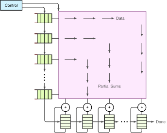
A 128 \(\times\) 128 systolic array capable of 16,384 operations per cycle requires a continuous operand stream to maintain utilization. On-chip buffers feed activations and weights to the array edges and are replenished from off-chip memory as needed; reuse within the array avoids fetching every operand from HBM each cycle. The TPU v4’s 1,200 GB/s HBM2 bandwidth helps sustain this stream, but off-chip bandwidth can still limit models whose working sets and reuse patterns exceed on-chip capacity.
Systems Perspective 11.1: Matching architecture to workload
Challenge: Systolic arrays must choose which operand to keep stationary in processing-element registers (weights, inputs, or partial sums), and that choice hard-codes the hardware’s preference for certain model types. Section 11.7.3 develops the three options as a general mapping decision.
No single accelerator architecture suits every workload. A chip optimized for weight-stationary dataflow (like early TPUs) excels at convolutional neural networks (CNNs), where filter weights are small and reused across many image patches. That same architecture stalls on large language model (LLM) autoregressive inference at batch size 1, where the entire weight matrix must be read from off-chip memory once per generated token with zero batch reuse. No choice of stationary operand recovers reuse that does not exist; the levers are batching, lower-precision weights, and memory bandwidth.
11.4.5 Numerics and sparsity on the datapath
Storing weights in INT8 or pruning half of them to zero shrinks a checkpoint on disk, but if the accelerator lacks a datapath that multiplies narrow integers or skips zero weights in silicon, the runtime must unpack those weights back to dense floating point and executes no faster than the baseline. Number formats and structured sparsity patterns were defined in Model Compression; what turns them into wall-clock speedups—including the ResNet-50 INT8 profile—is the hardware datapath that executes them. Systolic arrays and Tensor Cores often provision higher multiply-accumulate capacity for narrower formats such as FP16, BF16, INT8, and FP8, while halving or quartering the bytes moved per value relative to FP32. That speedup is not automatic: it requires a supported kernel, matching input and accumulation formats, and enough parallel work to keep the narrower datapath full without hitting another bottleneck.
Precision trade-offs
Lower precision is not free, for the range-and-precision reasons that forced loss scaling in mixed-precision training and that Numerical formats compared format by format. FP16 trades dynamic range for significand bits, BF16 keeps FP32’s exponent range at the cost of precision, and INT8 has no exponent at all, so its usable range depends on scale, zero-point, and clipping choices. For the hardware designer, those numerical properties set the silicon cost of each datapath. A narrower format needs a smaller multiplier and moves fewer bytes, but accumulation usually stays wider, as the FP32 accumulator of the Tensor Core instruction in listing 13 shows, so part of the area saved in the multipliers is spent keeping sums accurate.
↩︎ The software side of mixed-precision training, including loss scaling, is established in Mixed-precision training.
Precision support is integrated into execution units and memory paths. SIMD and SIMT lanes may support several scalar formats, while Tensor Cores (section 11.4.2) and systolic units (section 11.4.4) expose architecture-specific input and accumulation combinations. Changing storage alone may reduce bytes without producing the advertised arithmetic speedup, because the model must select a kernel that uses the efficient path. Converting FP32 weights to INT8 cuts weight traffic by 4\(\times\), but whether that moves a kernel from bandwidth bound to compute bound depends on the operation’s original arithmetic intensity, the ridge point of the accelerator’s INT8 path, and the overhead of quantization and dequantization (equation 10.4). Tiling and dataflow, not precision itself, determine reuse, while conversion, scaling, or fallback overhead can offset part of the gain. A format is useful only when the kernel and numerical policy can employ it safely.
Mixed-precision computing
Modern AI accelerators support mixed-precision execution, in which different stages of one computation use different numerical formats. The training recipe (FP16 or BF16 multiplications with FP32 accumulation) (Micikevicius et al. 2018; Mellempudi et al. 2019) is developed in Mixed-precision training, and the inference recipe (INT8 or INT4 weights with selected activations kept wider) in Numerical Precision: Changing How Values Are Stored. The hardware’s part is to execute several formats side by side, with an accumulator wide enough for each.
Micikevicius, Paulius, Sharan Narang, Jonah Alben, Gregory Diamos, Erich Elsen, David Garcia, Boris Ginsburg, et al. 2018. “Mixed Precision Training.” International Conference on Learning Representations (ICLR).
Mellempudi, Naveen, Sudarshan Srinivasan, Dipankar Das, and Bharat Kaul. 2019. “Mixed Precision Training with 8-Bit Floating Point.” arXiv Preprint arXiv:1905.12334.
NVIDIA. 2020b. TensorFloat-32 in the A100 GPU Accelerates AI Training, HPC up to 20x.
NVIDIA Corporation. 2017. NVIDIA Tesla V100 GPU Architecture. NVIDIA Whitepaper.
NVIDIA Corporation. 2018. NVIDIA Tesla T4 Tensor Core GPU. NVIDIA product documentation.
The shift toward precision diversity is evident in the evolution of AI hardware. Early architectures such as NVIDIA Volta provided Tensor Core support only for FP16, whereas later architectures, including Turing and Ampere, added integer formats and then TF32, a hybrid between FP32 and FP16, alongside BF16 (NVIDIA 2020b; NVIDIA Corporation 2017, 2018, 2020a). The generation-by-generation list of supported formats belongs with the other dated specifications in System Assumptions; the durable observation is the direction of the trend, toward more formats, each narrower than the last.
The precision format used in hardware design has cascading implications across the entire system. Reducing an operand from FP32 to FP16 halves its value bytes. When those values dominate traffic, the reduction can substantially lower movement energy; the full energy budget still includes access counts, arithmetic, and other device activity (Horowitz 2014). Simultaneously, Tensor Cores and systolic arrays can pack more lower-precision multiply-accumulate units into the same silicon area, raising peak throughput (Dally et al. 2021; Dally 2023). Lower-precision integer arithmetic also consumes less energy than FP32 in representative technology studies (Horowitz 2014), and the inference-focused TPUv1 was built around 8-bit multiply units (Jouppi et al. 2017). Reduced precision can therefore cut value traffic and raise the supported compute ceiling at the same time.
Kuzmin, Andrey, Mart Van Baalen, Yuwei Ren, Markus Nagel, Jorn Peters, and Tijmen Blankevoort. 2022. “FP8 Quantization: The Power of the Exponent.” Advances in Neural Information Processing Systems (NeurIPS), 14651–62. https://doi.org/10.52202/068431-1065.
Micikevicius, Paulius, Dusan Stosic, Neil Burgess, Marius Cornea, Pradeep Dubey, Richard Grisenthwaite, Sangwon Ha, et al. 2022. “FP8 Formats for Deep Learning.” arXiv Preprint arXiv:2209.05433.
Each narrower format raises the arithmetic ceiling again. The H100 advertises 989 TFLOP/s on its dense FP16 tensor path and 1,979 TFLOP/s on its FP8 path, an 8-bit floating-point format introduced for training and inference (Choquette 2023; Kuzmin et al. 2022; Micikevicius et al. 2022). NVIDIA’s Blackwell (B200) architecture extends this trajectory with an FP4 tensor datapath (a 4-bit floating-point format that, unlike INT4, spends some of its four bits on an exponent and so trades uniform spacing for range), rated at up to 9 PFLOP/s dense or 18 PFLOP/s sparse peak throughput per chip (NVIDIA Corporation 2024). Reaching those theoretical ceilings requires numerical representations, kernel implementations, and sparsity patterns that align exactly with the specialized hardware paths. Narrower numerical formats expand the available design space, but numerical stability and dynamic range requirements dictate whether a workload can safely use FP4.
N:M structured sparsity mechanics
The sparse rating in that comparison depends on one more datapath feature, one that skips zeros only when they follow a fixed pattern. While unstructured pruning reduces model parameter counts, it rarely translates to hardware speedup because arbitrary nonzero placements destroy memory locality. Hardware accelerators resolve this with N:M structured sparsity,18 the pruning constraint from model compression that keeps exactly \(\StructuredSparsityNonzeroCount\) of every \(\StructuredSparsityGroupSize\) contiguous values along the reduction dimension nonzero, so memory access stays uniform and indexing predictable across parallel execution units.
18 N:M structured sparsity: The 2:4 ratio (50 percent density) used by NVIDIA’s Ampere Sparse Tensor Cores is a hardware-friendly compromise: every contiguous four-value group retains two nonzero values, preserving regular indexing while halving the dense value payload (NVIDIA Corporation 2020a). At 2:4, the metadata overhead is compact enough to store alongside the weights without overwhelming the memory-traffic savings, which is the constraint that makes the advertised 2\(\times\) tensor-math throughput path plausible when kernels and model weights satisfy the pattern.
NVIDIA Corporation. 2020a. NVIDIA A100 Tensor Core GPU Architecture. NVIDIA Whitepaper, V1.0.
↩︎ The N:M and 2:4 structured sparsity patterns and their compressed storage are established in Structured pruning.
Parallel hardware needs this regularity because of how sparse matrices are encoded. Classical formats such as Compressed Sparse Row (CSR) and Block Compressed Sparse Row (BSR) rely on auxiliary index arrays to locate nonzero entries, and the corresponding activation gathers can touch scattered addresses, reducing useful bytes per memory transaction. Varying numbers of nonzeros across rows also create load imbalance and divergent execution. Block sparsity groups retained values into larger dense tiles to restore regularity, at the cost of a more restrictive pruning pattern. In the block formats, a short list of nonzero block indices tells the hardware which tiles to fetch, so zero blocks are never read. Whether an indexed format saves bytes or time at a given sparsity, its break-even point, is derived in Storage and execution break-even; the datapath question here is how regular the retained values must be for parallel hardware to use them.
↪ The CSR storage format is collected for reference in Sparse matrix formats.
NVIDIA. 2020a. Accelerating Matrix Multiplication with Block Sparse Format and NVIDIA Tensor Cores.
NVIDIA’s Sparse Tensor Cores implement the 2:4 instance of the N:M pattern (NVIDIA Corporation 2020a; NVIDIA 2020a). Their input is the compressed 2:4 encoding, the two retained values of each group plus a 4-bit metadata tag (2 bits per value) recording their original positions. During execution, the memory hierarchy transfers only the compressed weights and their metadata, halving the weight-value payload while adding metadata traffic; total transferred bytes therefore fall by less than half before other overheads. Inside the Sparse Tensor Core datapath, the 4-bit metadata steers an internal multiplexer network that selects the matching two values from an uncompressed four-element activation vector. These selected activations and the two nonzero weights are then routed into a half-sized dot-product multiplier tree. Because the hardware computes only on the nonzeros while streaming compressed weights, this design doubles the peak arithmetic instruction throughput, yielding an advertised 2\(\times\) tensor-math speedup over dense operations when weights are fine-tuned to satisfy the pattern (figure 6).
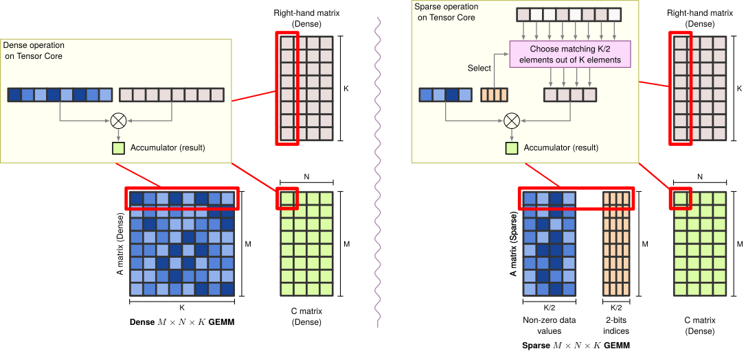
PyTorch. 2022. Accelerating Neural Network Training with Sparse Tensors.
The 2:4 pattern saves about half of the weight bytes and half of the multiplies, minus the metadata, so the reduced weight payload can lower traffic across HBM and on-chip SRAM. A roofline comparison must use consistent accounting: useful dense-equivalent operations can stay fixed while bytes decrease, whereas the count of physically executed sparse operations also decreases. Metadata and activation traffic remain in either traffic budget. Narrower values and skipped zeros therefore help when they reduce the bytes moved and keep the matrix engines fed, and the ResNet-50 INT8 profile collects that benefit only on an execution path that supports both its format and its shapes; how fast such a path can possibly run follows from one division.
Dividing a model’s total operation count by peak arithmetic throughput produces an idealized lower bound on execution time, not a realistic inference latency. On the H100’s INT8 tensor path, dividing ResNet-50’s 8.2 GFLOP per inference by the 1,979 TOPS peak yields a floor of about 4 μs, against 8 μs at the FP16 peak. Real single-image ResNet-50 inference takes far longer than either floor. Part of that gap is kernel launch, synchronization, and host overhead that no roofline captures; part is memory traffic in low-intensity layers, because bandwidth has improved more slowly than tensor arithmetic throughput. That imbalance decides whether the advertised INT8 peak delivers high sustained utilization or sits largely idle on a given workload (Horowitz 2014; Gholami et al. 2024), and closing the gap requires the other half of the anatomy: the memory hierarchy that supplies the compute units.
Self-Check: Question
In NVIDIA’s Ampere and Hopper architectures, how does 2:4 structured sparsity achieve an up to \(2\times\) dense-equivalent Tensor Core throughput path for supported matrix multiplication?
- Exactly two non-zero values are preserved in every contiguous four-element block, so the value payload is halved while compact metadata records positions and sparse Tensor Cores compute only on the retained values
- Every alternate row of the weight matrix is dropped completely, allowing the GPU to halve the grid launch dimensions
- Four separate threads simultaneously execute one scalar multiply-accumulate instruction in a single clock cycle
- Floating-point numbers are converted to 2-bit integers, quadrupling register file capacity
Place the following steps in the correct execution sequence for processing a matrix multiplication on an accelerator with Sparse Tensor Cores using 2:4 structured sparsity:
- Fine-tune or prune the weight matrix to ensure exactly two non-zero values exist in every four-element contiguous group
- Sparse Tensor Cores load compressed weights and decode metadata to gather matching input activation elements
- Multiply non-zero weights by gathered activations and accumulate into output partial sums on the sparse path
- Compress the sparse weight matrix by storing only the non-zero values alongside metadata describing their positions
What is the primary numerical difference between FP16 and BF16 as presented in this section?
- FP16 uses fewer total bits than BF16, so it always transfers less data
- BF16 has a wider exponent range, while FP16 has more fraction precision within the same 16-bit width
- FP16 is an integer format, whereas BF16 is floating point
- BF16 always prevents gradient underflow, whereas FP16 cannot be used for training
True or False: In NVIDIA’s SIMT (Single Instruction, Multiple Threads) execution model, when threads within the same 32-thread warp execute divergent branches of an
if-elsecondition, both paths are executed concurrently in parallel at full hardware throughput.
11.5 Memory Systems
A neural network kernel starves whenever the memory subsystem cannot deliver operands and consume outputs fast enough to saturate arithmetic pipelines. Modern accelerators provide hundreds of teraflops (or even petaflops) on low-precision tensor datapaths (NVIDIA Corporation 2020a, 2024; Choquette 2023), yet their compute pipelines idle as soon as memory traffic saturates the bus. This is the memory wall, the growing divergence between arithmetic capability and memory bandwidth, seen from inside the accelerator.
↩︎ The memory wall, the widening gap between compute growth and memory bandwidth growth, is established in Physical Constraints on Deployment.
Because deep neural networks manipulate millions or billions of parameters across high-dimensional activation tensors, performance is frequently dictated by data movement rather than raw arithmetic capacity. Accelerators combat this memory wall through tiered storage hierarchies, software-managed scratchpads, high-bandwidth 3D stacked memory, and architectural dataflow strategies designed to maximize spatial and temporal reuse. For the chapter’s ResNet-50 workload the question becomes where each activation tile lives between the moment one convolution writes it and the moment the next consumes it, and what each tier on that path costs in time and energy.
11.5.1 The AI memory wall
Upgrading to an accelerator with twice the peak FLOP/s yields zero speedup when a workload’s weights and activations already saturate memory bandwidth, pinning execution time at \(\frac{\DataVolume}{\Bandwidth}\). On an accelerator the AI memory wall is chiefly this bandwidth ceiling, set by the parameter volumes and activation tensors of deep learning rather than by the single-access latency gap of the classic CPU formulation. Adding more memory capacity does not remove it either, because a model that fits comfortably in device memory still waits on the rate at which its bytes reach the compute units of section 11.4. The energy side of the wall was set out with the energy ladder in section 11.2.3: an off-chip DRAM access costs about 173× the energy of the FP32 multiply that consumes its operand (figure 4), and the memory wall adds the time side of the same imbalance, which grows with every hardware generation.
Quantifying the compute-memory performance gap
Over the past two decades, peak computational capabilities have grown substantially faster than DRAM bandwidth (Gholami et al. 2024). This divergence stems from physical scaling constraints: while transistor scaling and dense systolic arrays multiply arithmetic throughput, memory bandwidth remains bounded by pin counts, package-substrate routing density, and interface signaling power. Representative high-end accelerators can deliver on the order of \(10^3\) TFLOP/s of peak tensor throughput (for example, NVIDIA H100 delivering 989 TFLOP/s in FP16 or 1,979 TFLOP/s in dense FP8) while providing approximately 3.35 TB/s of memory bandwidth (Choquette 2023). This implies that on the order of \(10^2\) FLOP of work per byte moved is required to fully use the compute, a threshold section 11.6.2 calls the ridge point and that exceeds the arithmetic intensity of many practical neural network workloads.
When a workload’s arithmetic intensity falls below this threshold, data transfer (\(\frac{\DataVolume}{\Bandwidth}\)) sets the larger of the two modeled time bounds. Accelerators attempt to tolerate memory latency (typically hundreds of clock cycles for off-chip DRAM) by maintaining thousands of concurrent execution threads and switching between active warps while memory requests remain in flight. However, when memory bandwidth saturates or when register pressure limits occupancy, the scheduler runs out of independent instructions to issue. Compute pipelines then stall, leaving high-throughput tensor cores idle while waiting for operands. Simultaneously, driving wide off-chip memory buses across capacitive printed circuit board traces and PHY interfaces consumes a substantial fraction of the chip’s thermal design power (TDP), directly constraining the energy budget available for arithmetic logic (Horowitz 2014; Sze et al. 2017).
The time gap and the energy ladder describe the same pressure from two sides: each byte fetched from DRAM costs more time relative to the arithmetic it feeds with every generation, on top of its energy cost. The TPUv1’s performance-per-watt advantage (example 11.1) came largely from minimizing that off-chip movement through systolic arrays and large on-chip SRAM (Jouppi et al. 2017). Whether a model can exploit such a design depends on the pattern of its memory accesses, which differs sharply among parameters, activations, and optimizer state.
Krizhevsky, Alex, Ilya Sutskever, and Geoffrey E. Hinton. 2012. “ImageNet Classification with Deep Convolutional Neural Networks.” Advances in Neural Information Processing Systems (NeurIPS) 25.
Simonyan, Karen, and Andrew Zisserman. 2015. “Very Deep Convolutional Networks for Large-Scale Image Recognition.” arXiv Preprint.
Chowdhery, Aakanksha, Sharan Narang, Jacob Devlin, Maarten Bosma, Gaurav Mishra, Adam Roberts, Paul Barham, et al. 2022. “PaLM: Scaling Language Modeling with Pathways.” arXiv Preprint arXiv:2204.02311.
Dubey, Abhimanyu, Abhinav Jauhri, Abhinav Pandey, Abhishek Kadian, et al. 2024. The Llama 3 Herd of Models. arXiv preprint arXiv:2407.21783.
DeepSeek-AI. 2025. “Insights into DeepSeek-V3: Scaling Challenges and Reflections on Hardware for AI Architectures.” Proceedings of the 52nd Annual International Symposium on Computer Architecture, 1731–45. https://doi.org/10.1145/3695053.3731412.
NVIDIA Corporation. 2024. NVIDIA Blackwell Architecture. NVIDIA product documentation.
AMD. 2023. AMD Instinct MI300X Accelerators. AMD product documentation.
Hardware balance is the supply side of the memory wall; model size is the demand side. The structural widening between model footprints and available memory bandwidth is what turns the iron law’s memory term into the binding constraint across generations. Parameter count is a capacity quantity. In low-batch dense decoding with weights streamed from device memory, weight traffic per generated token grows with the parameter count. Sparse expert models read selected experts rather than every stored parameter, so their total parameter counts do not directly specify per-token traffic. Figure 7 plots this logarithmic divergence relative to 2014, contrasting the roughly 3,900× increase in dense model parameters (filled red points) against the 33× increase in per-device accelerator memory bandwidth (blue points) to isolate the widening shaded memory-wall gap (Krizhevsky et al. 2012; Simonyan and Zisserman 2015; Brown et al. 2020; Chowdhery et al. 2022; Dubey et al. 2024). DeepSeek-V3 appears as an open marker at its total parameter count and is left out of the trend for exactly that reason (DeepSeek-AI 2025). Even high-bandwidth accelerators such as NVIDIA B200 and AMD MI300X/MI325X cannot close this growth-rate gap through bandwidth scaling alone (NVIDIA Corporation 2024; AMD 2023). Parameter counts for proprietary systems such as GPT-4 and Gemini are not officially disclosed, so they are not plotted as factual data points.
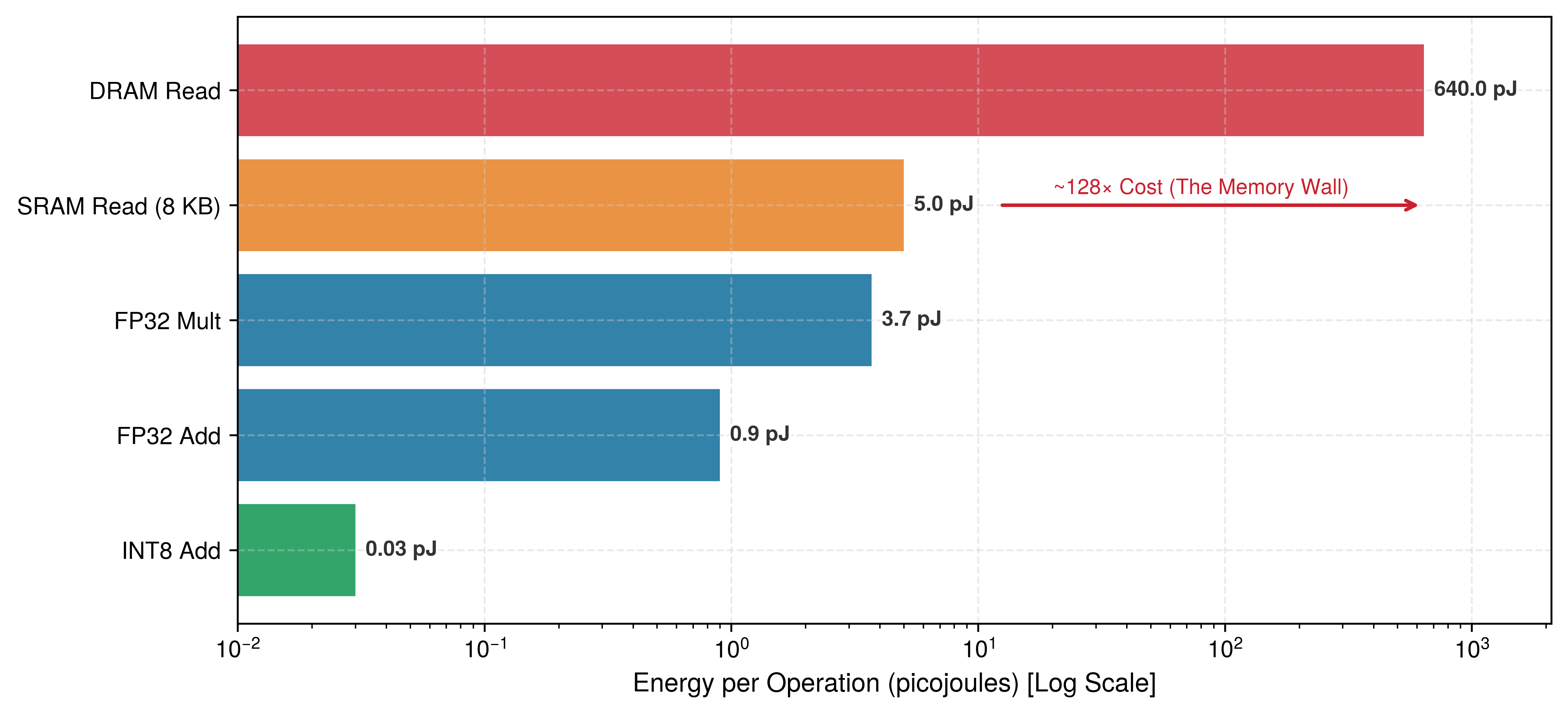
Gholami, Amir, Zhewei Yao, Sehoon Kim, Coleman Hooper, Michael W. Mahoney, and Kurt Keutzer. 2024. “AI and Memory Wall.” IEEE Micro 44 (3): 33–39. https://doi.org/10.1109/mm.2024.3373763.
11.5.2 Memory access patterns in ML workloads
In dense FP16 autoregressive generation at batch size 1, streaming a model’s weights from device memory for each generated token yields roughly 1 FLOP/byte on the matrix-vector work, starving compute units before activations or gradients ever enter the picture. Across training and inference, parameters, activations, and optimizer states compete for that same memory bandwidth in distinct ways. Model parameters (weights and biases) can span hundreds of billions of values (Brown et al. 2020) that must stream from memory whenever batch reuse is low. Intermediate activations produced at each layer must also be buffered for subsequent operations, and during training those forward activations must either stay in memory until backpropagation consumes them or be recomputed on the backward pass. Training then compounds the traffic with gradients and optimizer state: backpropagation writes a gradient for every parameter, and adaptive optimizers such as Adaptive Moment Estimation (Adam) read and write multi-word momentum states on every step, multiplying the bytes moved per parameter update (Narayanan et al. 2021; Kwon and Rhu 2018).
Brown, Tom B., Benjamin Mann, Nick Ryder, Melanie Subbiah, Jared Kaplan, Prafulla Dhariwal, Arvind Neelakantan, et al. 2020. “Language Models Are Few-Shot Learners.” Advances in Neural Information Processing Systems 33: 1877–901. https://doi.org/10.48550/arxiv.2005.14165.
Kwon, Youngeun, and Minsoo Rhu. 2018. “TensorDIMM: A Practical Near-Memory Processing Architecture for Embeddings and Tensor Operations in Deep Learning.” Proceedings of the 52nd Annual IEEE/ACM International Symposium on Microarchitecture, 740–53. https://doi.org/10.1145/3352460.3358284.
The physical cost of this data movement depends on where each tensor resides in the memory hierarchy. While an on-chip register access completes in a single clock cycle at sub-picojoule energy, a dependent off-chip DRAM fetch can expose hundreds of cycles of latency and expends orders of magnitude more energy. Independent requests can overlap that latency, subject to available concurrency and bandwidth. Tracing a single tensor of the chapter’s ResNet-50 workload through the memory tiers during an inference pass makes this disparity concrete (lighthouse 11.2).
Lighthouse 11.2: Life of a tensor: A ResNet-50 activation map
Follow one activation map of the chapter’s ResNet-50 workload, the output of a stage-2 convolution (\(56{\times}56\) positions by 64 channels), on its way to the next convolution’s Tensor Cores on an H100:
- HBM: The previous kernel wrote the map here.
- Size: 201 KB per image at INT8 and 401 KB at FP16; a batch of 32 holds 6.4 MB at INT8.
- Latency: A dependent off-chip request takes about 300 ns, while streaming one image’s map at full bandwidth would take only about 60 ns, so the kernel must keep many requests in flight to approach the bandwidth ceiling.
- Energy: About 160 pJ per byte in the 45 nm estimates used throughout the chapter, or about 32.1 µJ to read one image’s map once.
- L2 cache: The H100 shares 50 MB of L2 across its streaming multiprocessors (SMs), enough to hold the whole batch’s map at INT8 if the next kernel consumes it soon after the previous one wrote it.
- Latency: About 150 ns on Hopper.
- Shared memory: One SM stages a tile of the map in its 228 KB of software-managed shared memory. A whole image’s map fits at INT8 but not at FP16, so the INT8 format changes which tier can hold it.
- Latency: About 17 ns on Hopper.
- Registers: The Tensor Core reads its operands here.
- Latency: A small number of cycles, depending on the instruction.
- Energy: About 0.1 pJ per access, more than three orders of magnitude below an off-chip access.
- Device arithmetic peak: 1,979 TOPS on the H100 INT8 tensor path, the rate these registers must sustain, not a register-transfer rate.
Systems insight: Latency and energy per access rise from registers to HBM. The working set’s location, access count, reuse, and dependencies determine the memory contribution to time and energy; arithmetic adds its own cost. The bandwidth term of the roofline is whichever link of this ladder the working set must cross; HBM-to-L2 is one possible limiting link, not the only one.
The boundary between bandwidth-bound and compute-bound execution emerges directly from the balance between data transfer time and arithmetic execution time. For a workload requiring data volume \(\DataVolume\) (bytes) across available memory bandwidth \(\Bandwidth\) (bytes/s), and executing \(\Operations\) floating-point operations on hardware with peak throughput \(\PeakRate\) (FLOP/s) at realized hardware utilization \(\EfficiencyHw\), the respective execution times are the iron law’s data and compute terms: \[\begin{gather*} \IronlawTermTimesMemory = \frac{\DataVolume}{\Bandwidth} \\ \IronlawTermTimesCompute = \frac{O}{\PeakRate \cdot \EfficiencyHw} \end{gather*}\]
In a strictly sequential model without overlap, \(\IronLawMemoryTime > \IronLawComputeTime\) identifies bandwidth-bound execution. When hardware overlaps memory transfers with computation, the larger term sets the theoretical lower bound on execution time. In practice, however, data dependencies, memory controller queueing, and partial pipeline overlap dictate how much arithmetic hardware remains idle while waiting for operands.
Irregular memory access
Production machine learning workloads combine regular dense matrix kernels with irregular memory access patterns that defeat conventional caching and prefetching hardware. While dense operations like general matrix multiply (GEMM) and convolution stream contiguous blocks that map cleanly onto hardware caches and systolic arrays, irregular operations rely on indirect, sparse, or input-dependent memory addresses. Table 5 contrasts these two memory regimes across access geometry, cache locality, and hardware pressure.
| Feature | Regular dense kernels | Irregular ML components |
|---|---|---|
| Access pattern | Contiguous or tiled | Indirect, scattered, or input-dependent |
| Cache locality | Often high after tiling | Often lower and workload-dependent |
| Data reuse | Structured across tiles or batches | Sparse or dynamic, depending on the operator |
| Dependencies | Static loop nests | Input-dependent routing or variable shapes |
| Examples | GEMM, convolution, dense attention | Embedding lookup, unstructured sparsity, MoE routing |
| Primary pressure | Compute or bandwidth, depending on arithmetic intensity | Latency, bandwidth, metadata, and load imbalance |
| Energy consequence | Depends on reuse and memory tier | Extra movement and metadata can increase energy |
Within a single neural network, memory access behavior varies sharply across layer types. Convolutional layers have high spatial locality and register reuse as small weight kernels slide across input feature maps, whereas fully connected layers and dense attention execute regular matrix multiplications whose large parameter matrices or key-value caches can exceed on-chip SRAM capacity and become bandwidth bound when operational reuse is low. Variable sequence lengths complicate memory buffer allocation, yet the attention operations within each sequence remain regular, contiguous matrix multiplies.
True memory irregularity arises instead from unstructured sparsity,19 embedding lookups, and dynamic token routing. Unstructured sparsity stores nonzero weights or activations in compressed formats (such as CSR or COO) that require pointer indirection to decode operand coordinates. Embedding tables break sequential transfers in a different way: sparse categorical IDs select arbitrary rows from tables spanning tens of gigabytes in DRAM, turning reads into uncoalesced, scattered fetches. DLRM, the book’s capacity-bound lighthouse, is the extreme case, because its embedding tables exceed one accelerator’s memory and each lookup fetches a short row from an address known only when the input arrives, defeating both caches and prefetchers. Mixture-of-Experts (MoE) models introduce a third irregularity at the routing layer, where gates direct tokens to different expert networks based on input context; although deterministic for a given input, token assignments vary across batches, disrupting prefetch pipelines and unbalancing execution queues across parallel cores.
19 Sparsity and memory irregularity: Unstructured sparse formats commonly gather nonzero elements through indirect addressing, which can weaken sequential access and make metadata overhead significant. Structured sparsity preserves hardware-friendly blocks, so its access behavior differs from arbitrary pruning. Without suitable kernels or hardware support, an unstructured sparse model can run slower than its dense counterpart despite performing fewer arithmetic operations.
Irregularity degrades performance through distinct mechanisms, and treating them as one memory problem can point to the wrong optimization. Scattered addresses may turn one logical access into several memory transactions, so each fetched cache line carries few useful payload bytes. Indirection can also serialize address generation: the system must fetch an index or pointer before it knows which payload to request, limiting memory-level parallelism even when aggregate bandwidth remains available. Input-dependent routing creates a third failure mode when some processing elements receive longer queues than others; completion time follows the slowest queue while neighboring units idle. Variable-sized allocations may fragment capacity, but fragmentation is neither necessary nor sufficient for irregular access. A sequential stream can saturate bandwidth without being irregular, whereas a dependent lookup chain can stall far below peak bandwidth.
Diagnosis should therefore begin with the mechanism that prevents forward progress. A low ratio of useful payload bytes to transferred bytes indicates poor spatial utilization or coalescing. Long memory stalls alongside unused bandwidth indicate dependent misses or too few concurrent requests to hide latency. Uneven queue depths or per-route work reveal load imbalance rather than a cache-capacity problem. Cache hit rate alone cannot distinguish these cases because a miss can waste bandwidth, expose latency, or both. Each diagnosis implies a different remedy: packing or blocking improves spatial utilization, reordering and prefetching expose concurrent requests, structured sparse formats reduce indexing overhead, and routing or partitioning balances work. The memory hierarchy determines the cost of the remaining accesses, while dataflow and tensor-layout choices determine how much irregularity software can remove before execution reaches the hardware.
The optimization order follows that diagnosis. Representation comes first when the format is under system control because a block-structured sparse format or grouped routing can remove indirection before a kernel executes. Request organization comes next: accesses issued together should target adjacent addresses, and enough independent requests must remain in flight to hide unavoidable latency. Additional cache capacity or bandwidth helps only when profiling shows that the regularized request stream still exhausts that resource. More bandwidth cannot resolve a serial pointer dependency, and more capacity cannot rebalance skewed work. The objective is to expose as much regular structure as possible while confining unavoidable irregularity to the smallest portion of execution.
Software can mitigate irregular access by regularizing tensor layouts, enforcing structured sparsity, and sorting dynamic routes into uniform batches. Yet software restructuring cannot eliminate the physical penalty of data movement: whether a memory request is contiguous or scattered, every transferred byte must cross physical wires governed by finite bandwidth, propagation latency, and energy dissipation. Bounding these physical costs requires organizing storage into cascading hardware tiers. Rather than treating memory as a uniform pool, accelerator architectures deploy multilevel memory hierarchies that trade off capacity against latency and energy at every tier.
11.5.3 Memory hierarchy
No single storage technology can simultaneously satisfy the multi-terabyte-per-second bandwidth required by dense execution units and the tens of gigabytes of capacity required to hold modern model parameters. Accelerators resolve this tension through multilevel memory hierarchies. Rather than treating memory as a monolithic address space, the machine organizes storage into distinct physical tiers, each optimized for a specific balance of capacity, access latency, bandwidth, and energy dissipation.
At the apex of the hierarchy, register files and on-chip SRAM caches supply operands to arithmetic units with sub-nanosecond latency and single-digit picojoule energy costs, but their capacity is strictly limited by silicon die area. At the base, nonvolatile flash storage holds hundreds of gigabytes of model checkpoints and training datasets, but requires milliseconds or microseconds to access. Between these boundaries, software-managed scratchpads stage active tensor tiles, while device-local DRAM (such as HBM or GDDR) provides the primary working memory for parameters and activations.
This organization establishes an inverse relationship across tiers: as storage capacity expands and physical distance from arithmetic units grows, bandwidth falls, latency lengthens by orders of magnitude, and energy consumption per bit escalates. Table 6 compares these tiers across latency, bandwidth, capacity, and functional roles in deep learning workloads.
| Memory Level | Relative latency | Bandwidth | Relative capacity | Example Use in Deep Learning |
|---|---|---|---|---|
| Registers | Lowest | Highest | Tiny | Storing operands for immediate computation |
| L1/L2 Cache (SRAM) | Very low | High | Small | Caching frequently accessed activations and small weight blocks |
| Scratchpad memory | Very low | High | Small to medium | Software-managed storage for intermediate computations |
| Device DRAM (HBM, GDDR, or LPDDR) | High | Moderate–Very High | Large | Storing model parameters and activations that do not fit on-chip |
| Host DRAM (typically DDR) | High locally; transfer adds latency | Moderate | Large to very large | Staging or offloading data outside accelerator memory |
| Flash Storage (SSD/NVMe) | Very high | Low | Very large | Storing pretrained models and checkpoints for later loading |
A recurring systems question is why accelerators cannot bypass on-chip SRAM entirely and stream all operands directly from high-capacity off-chip DRAM. A dependent DRAM request exposes the full access latency. Many independent requests can hide that latency, but their sustained operand supply remains limited by off-chip bandwidth; on-chip staging also enables reuse.
Napkin Math 11.2: Why HBM cannot feed the array directly
Problem: Why is on-chip SRAM necessary instead of fetching all data from HBM?
Math:
- Clock cycle: At 2 GHz, \(1/(2\text{ GHz}) = 500\text{ ps}\).
- DRAM access: Off-chip HBM sits millimeters away on the package, but row activation, DRAM-array latency, serialization, protocol traversal, and queuing add up to 100+ cycles per access.
- Distance, for comparison: On an H100-class 814 mm² die, signals travel ~20 mm; at \(\approx 0.5\VacuumLightSpeed\), \(20\text{ mm}/(0.5\VacuumLightSpeed) \approx 130\text{ ps}\), less than one cycle.
Systems insight: The propagation estimate alone does not explain the DRAM access cost, and it omits real interconnect delay from wiring and routing. Independent requests can overlap the 100-plus-cycle access path; a dependent request cannot. Registers and SRAM supply operands at the rate the array needs while reusing values that would otherwise cross HBM repeatedly. Transformer tiling addresses both operand supply and reuse, whereas streaming a growing KV cache can still limit inference when its required traffic exceeds the available bandwidth.
On-chip memory
The on-chip memory subsystem integrates registers, Static Random-Access Memory (SRAM) caches, and software-managed scratchpads directly on the accelerator die. Register files provide the immediate operand and accumulator storage needed by execution pipelines. Modern accelerators provision substantial register capacity in aggregate across the chip, but partition this pool dynamically among concurrent threads or warps. Increasing per-thread register allocation allows individual threads to retain larger matrix tiles, but limits the total number of concurrently scheduled warps, reducing the hardware’s ability to hide memory latency. Conversely, underallocating registers forces the compiler to spill values to off-chip memory, converting single-cycle register accesses into multi-cycle stalls. Efficient kernel design balances register allocation to maintain maximum occupancy while keeping hot operands resident.
Hardware-managed L1 and L2 caches provide fast buffering for frequently referenced data using automatic tag checking and hardware eviction policies. However, automatic caches are poorly suited for streaming multi-gigabyte tensor operations: scanning through large activation tensors can evict reusable weight tiles before arithmetic units can reuse them. Furthermore, specialized execution pipelines impose strict layout and data-type constraints that general caches cannot satisfy automatically. As illustrated in example 11.3, hardware matrix engines require specific alignments and memory layouts; a mismatch may require padding, conversion, or a different kernel whose efficiency must be checked.
Example 11.3: Tensor Cores that never engage
Scenario: An engineering team migrates a transformer workload to NVIDIA A100 GPUs expecting automatic Tensor Core acceleration, but profiling reveals Tensor Cores remain idle (NVIDIA Corporation 2020a).
Diagnosis: The workload used shapes and data types that selected less efficient kernels rather than the intended Tensor Core path.
Systems lesson: Specialized paths have operator, precision, layout, and shape requirements. Libraries can often handle nonaligned dimensions through padding or alternative kernels, but reaching high utilization requires verifying which path was actually selected.
To avoid the eviction overhead and unpredictability of automatic caches, AI accelerators incorporate scratchpad memory. Unlike hardware caches, scratchpads are software-managed SRAM structures mapped directly into the core’s address space without tag directories or hardware replacement logic. The compiler or programmer explicitly controls when tensor tiles are loaded from external DRAM, how long they reside on-chip, and when updated values are written back. In convolutional models, scratchpads retain input feature maps and weight kernels across sliding receptive windows, eliminating redundant DRAM reads (Chen et al. 2017). On NVIDIA GPUs, scratchpad memory is exposed as shared memory: a fast, programmer-controlled SRAM bank shared across all threads within a thread block. Custom kernels written in CUDA or Triton manage shared memory explicitly. FlashAttention demonstrates the power of this mechanism: rather than materializing the full \(\SequenceLength{\times}\SequenceLength\) attention score matrix in off-chip HBM, the kernel tiles queries, keys, and values through shared memory and updates softmax statistics online (Dao et al. 2022). The speedup stems entirely from eliminating high-latency HBM round trips rather than reducing arithmetic operations; in fact, the algorithm recomputes intermediate attention values during the backward pass to avoid storing them to off-chip memory.
↩︎ FlashAttention as an IO-aware attention kernel for training is established in FlashAttention: IO-aware attention optimization.
Off-chip memory
When tensor working sets exceed on-chip SRAM capacity, operands and parameters reside in device-local DRAM. Rather than sequential hierarchy levels, HBM, Graphics DDR (GDDR), and Low-Power DDR (LPDDR) represent alternative memory architectures engineered for distinct cost, bandwidth, and power envelopes. High-performance accelerators use HBM, which stacks DRAM dies vertically using through-silicon vias (TSVs) and interfaces with the accelerator die across a wide silicon interposer (e.g., 1,024 to 8,192 bits). This wide bus delivers multi-terabyte-per-second bandwidth at lower clock frequencies and lower energy per bit than conventional DRAM, but requires complex 2.5D packaging. Where silicon interposers are cost-prohibitive, accelerators adopt GDDR, which uses narrower buses (e.g., 256 to 384 bits) driven at high pin speeds across standard circuit boards. Mobile and embedded accelerators use LPDDR, trading raw bandwidth for low operating voltage and reduced standby power.
When parameter and activation footprints exceed device-local DRAM capacity, the system must offload state to host DRAM (typically standard DDR). Accessing host memory requires crossing an I/O interconnect such as PCIe or a coherent fabric like NVLink or Compute Express Link (CXL). Because PCIe bandwidth (tens of gigabytes per second) is one to two orders of magnitude lower than accelerator DRAM bandwidth, unmanaged offloading stalls arithmetic execution. Efficient runtimes mitigate this penalty by overlapping asynchronous direct memory access (DMA) copies with kernel execution, prefetching upcoming layer parameters while current layers compute.
At the base of the hierarchy, nonvolatile flash storage and solid-state drives (SSDs) provide persistent, multi-terabyte capacity for datasets and training checkpoints (Narayanan et al. 2021). With read latencies measured in tens of microseconds and bus bandwidths capped at single-digit gigabytes per second, flash devices cannot participate directly in kernel execution. Checkpointing and data-loading pipelines treat flash storage as an asynchronous streaming source, staging batches through host DRAM into accelerator memory before computation begins.
Narayanan, Deepak, Mohammad Shoeybi, Jared Casper, Patrick LeGresley, Mostofa Patwary, Vijay Korthikanti, Dmitri Vainbrand, et al. 2021. “Efficient Large-Scale Language Model Training on GPU Clusters Using Megatron-LM.” Proceedings of the International Conference for High Performance Computing, Networking, Storage and Analysis, 1–15. https://doi.org/10.1145/3458817.3476209.
The physical tiers of the memory hierarchy establish the latency floors and capacity ceilings of the accelerator, but advertised memory bandwidth is only a ceiling within them; achievable bandwidth depends on access pattern, batching, locality, and the host interface that feeds the accelerator. Peak figures assume continuous, stride-1 coalesced access across all memory channels. Real neural network workloads deviate substantially from this ideal: transformer attention, convolution, and fully connected layers realize distinct fractions of peak bandwidth because their memory access strides, tiling dimensions, and operational reuse differ. A sufficiently large, coalesced weight stream can approach peak bandwidth even at small batch size. Batching instead reuses each loaded weight across more samples, raising arithmetic intensity as analyzed under the roofline model in section 11.6. Small or irregular kernels may lack enough concurrent accesses to approach the bandwidth ceiling, making memory latency and available parallelism part of the diagnosis.
11.5.4 Host-accelerator communication
An accelerator rated for hundreds of teraflops sits idle if its input tensors are still crawling across a host PCIe bus an order of magnitude slower than its on-package HBM. In discrete accelerator systems, the host CPU and the accelerator operate as separate computational domains joined by a peripheral bus: the host manages storage I/O, network streams, and runtime orchestration in system DRAM, while the accelerator executes dense mathematical kernels over device memory (HBM or GDDR). Because those two memories occupy separate physical address spaces, computation cannot begin until tensors cross the host-accelerator interconnect, making peripheral bus bandwidth and launch latency a hard gate on end-to-end speedup.
Figure 8 sequences the four-stage execution trace across host and device lifelines: copying input data across PCIe to device memory via DMA (step 1), dispatching kernel instructions from the CPU (step 2), executing parallel core compute with local writeback (step 3), and copying results back to host memory (step 4). In a naive synchronous execution model, every transfer step sits directly on the critical path, stalling either the host or the accelerator until each memory transaction finishes.
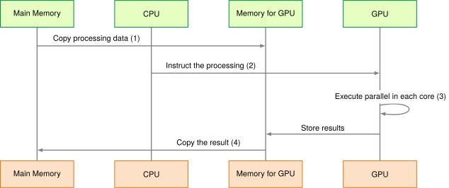
The end-to-end latency of a kernel launch decomposes into transfer time, queue dispatch overhead, and arithmetic execution time. When tensor transfers are small or frequent, the fixed overhead of driver submission and bus round trips dominates runtime. When transfers are large, the low bandwidth of PCIe relative to on-package HBM creates a sustained I/O bottleneck. In D·A·M terms, the Machine boundary between host and accelerator forces the Algorithm to maximize arithmetic reuse on the device once tensors arrive.
Node-level interconnect topology
Within a single machine, how bits move between GPUs and the CPU sets the next ceiling. In the 1–8 GPU regime, scaling is achieved through high-speed intra-node interconnects such as NVLink and host-to-device PCIe transfers that mitigate the memory wall. These links form a bandwidth taper: data-movement speed falls at each step away from the compute units, from on-package HBM through the GPU-to-GPU NVLink bridge down to the host PCIe link. The PCIe step is much slower than the accelerator-local memory and inter-GPU fabric, so any data path that touches the CPU can become a performance hazard, and keeping accelerator-to-accelerator traffic off that link is the reason NVLink exists (NVIDIA Corporation 2020b). A typical AI server is therefore not a flat mesh of connected devices, and optimizing data movement starts from its physical topology.

Bandwidth tapers steeply as data moves farther from the accelerator.
Within a multi-accelerator server node, two interconnect tiers define this bandwidth taper below device memory:
- Device-device interconnect (NVLink/Infinity Fabric): Modern multi-GPU nodes use specialized high-speed bridges like NVLink20 to connect accelerators directly, bypassing the host CPU. Bandwidth ranges from 600 GB/s to 900 GB/s per GPU (NVIDIA Corporation 2020b; Choquette 2023). This link matters whenever tensors must move between accelerators within one server, including model partitioning, activation exchange, and gradient synchronization during training. The architectural principle is the boundary: traffic that stays on the accelerator fabric is far cheaper than traffic that falls back through the host.
- Host-device interconnect (PCIe): The link between the CPU and the accelerator. Bandwidth ranges from 32 to 64 GB/s (PCIe Gen4/Gen5). Host-staged training data can bottleneck here, although resident data, direct storage or network I/O, and coherent accelerator links can use other paths. Multi-GPU servers may also provide multiple PCIe links rather than a single shared 64 GB/s path.
20 NVLink (NVIDIA Link): This direct GPU-to-GPU interconnect exists to keep accelerator-to-accelerator traffic off PCIe when tensors must move inside a server. Its 600–900 GB/s aggregate bidirectional bandwidth is roughly 300–450 GB/s per direction under balanced full-duplex traffic, several times the directional bandwidth of a standard PCIe link, so workloads with frequent cross-device tensor movement can remain in the fast part of the bandwidth taper (NVIDIA Corporation 2020b; Choquette 2023). Training algorithms determine how much tensor traffic must cross this link; the hardware fact needed here is the bandwidth gap.
NVIDIA Corporation. 2020b. “NVLink: Scalable High-Performance Interconnect.” NVIDIA Technical Report 2020.
Choquette, Jack. 2023. “NVIDIA Hopper H100 GPU: Scaling Performance.” IEEE Micro 43 (3): 9–17. https://doi.org/10.1109/mm.2023.3256796.
A third tier, the network link from one server to others, continues the taper beyond the node (section 11.9). Together the levels produce a characteristic bandwidth taper:
\[\begin{aligned} \text{HBM (3350 GB/s)} &\gg \text{NVLink (900 GB/s)} \\ &\gg \text{PCIe (64 GB/s)} > \text{Network (50 GB/s)} \end{aligned}\]
System efficiency depends on keeping tensors on the highest-bandwidth links available. Because PCIe and network links offer orders of magnitude less bandwidth and higher latency than on-package memory, placement and scheduling must minimize crossings across these boundaries.
Transfer optimization
The standard remedy for transfer overhead is the asynchronous pipeline of Devices and memory. Batches staged in pinned (page-locked) host memory are copied by dedicated DMA engines while the accelerator computes on the previous batch. This double buffering conceals transfer latency behind arithmetic runtime whenever computation time exceeds transfer time (\(\IronLawComputeTime \ge \BatchTransferTime\)). When compute duration is too short to amortize the transfer, execution remains bus bound and the compute units stall.
↩︎ The feeding problem, in which data delivery fails to keep pace with compute throughput, is established in The feeding problem.
Unified Memory takes the opposite approach, presenting a single virtual address space that spans host DRAM and device HBM while the driver migrates pages on demand whenever either processor touches an address. On-demand migration removes staging code at the cost of predictability, because each page fault stalls execution and scattered accesses can thrash pages across the PCIe bus. High-throughput production workloads therefore rely on explicit, pipelined DMA transfers and reserve Unified Memory for prototyping or for applications where programmer productivity outweighs sustained hardware utilization.
11.5.5 Model memory pressure
An optimization that relieves memory pressure for one model family can leave another untouched: caching weights helps nothing when ResNet-50’s early convolutions spill large activation maps to DRAM, and spatial activation tiling helps nothing when GPT-2 decode streams gigabytes of weights for a single token. Model architecture determines which memory term binds. The architectural reasons each family stresses memory as it does were traced in Arithmetic intensity across workloads; the hardware consequence differs by family, and the lighthouse models of Lighthouse Models as Reference Workloads cover the cases.
Dense layers, the multilayer perceptron (MLP) blocks that every family contains, are bound by weight traffic at small batch. At batch size \(\BatchSize= 1\), each parameter loaded from off-chip memory serves a single multiply-accumulate operation (often \(\le 1\text{ FLOP/byte}\)), so execution sits on the bandwidth slope; batching reuses each loaded weight across \(\BatchSize\) inputs and moves the layer toward the compute ceiling. Dense weight matrices regularly exceed the tens of megabytes of on-chip SRAM, so parameters reside in HBM and stream through tiles that the accelerator double-buffers into SRAM (Chen et al. 2017). The host link enters the critical path only when inputs stream from the host or when the model exceeds device memory.
Chen, Yu-Hsin, Joel Emer, and Vivienne Sze. 2017. “Using Dataflow to Optimize Energy Efficiency of Deep Neural Network Accelerators.” IEEE Micro 37 (3): 12–21. https://doi.org/10.1109/mm.2017.54.
Convolutional layers, the core of ResNet-50, place their memory pressure on activations rather than weights. Small filters sliding across feature maps supply three forms of reuse: neighboring windows share input activations, each filter is applied at every spatial position, and each input channel feeds every output filter. Early layers therefore carry compact parameter tensors but large activation maps that exceed on-chip SRAM, and unoptimized layer-by-layer execution spills those maps to device DRAM. Spatial tiling keeps activation tiles, with their overlapping boundary pixels, in on-chip buffers so adjacent convolutions consume them without refetching (Chen et al. 2017).
Transformers such as GPT-2 stress both capacity and bandwidth, differently in each phase. During training and prefill, standard attention materializes an \(\SequenceLength{\times}\SequenceLength\) score matrix for sequence length \(\SequenceLength\) and moves \(\mathcal{O}(\SequenceLength^2)\) bytes through HBM; IO-aware kernels such as FlashAttention (Dao et al. 2022) keep those tiles in on-chip SRAM instead (FlashAttention: IO-aware attention optimization). During autoregressive decode, each generated token reads the weights and the accumulated key-value (KV) cache from HBM for a vector-matrix product, which binds generation speed to memory bandwidth.
↩︎ How much memory one request’s KV cache claims as its sequence grows is established in Autoregressive decoding.
Two other lighthouses stress memory in other ways: DLRM’s sparse embedding lookups stress random-access bandwidth rather than dense compute, and MobileNetV2’s depthwise convolutions trade arithmetic intensity for a smaller parameter footprint, so both reappear as memory-bound rows in the roofline operations table (table 7). Accelerators answer these divergent demands with the tiered hierarchy. On-chip SRAM captures high-reuse activations and tiled matrix blocks at tens of terabytes per second, HBM stages large weight tensors and sequence state, and NVLink-class links carry tensors between accelerators when a model exceeds one device, avoiding the narrower host PCIe bus. Table 14 later pairs each family’s memory profile with the mapping that answers it. Because a reference off-chip DRAM access costs far more energy per event than arithmetic (figure 4), reducing repeated external accesses improves efficiency, but deciding whether a given kernel is limited by compute throughput or by memory bandwidth requires an analytical boundary. The roofline model supplies that boundary by comparing operational intensity against hardware performance limits, so that optimization effort targets the resource that actually binds.
Self-Check: Question
When training a \(7\)-billion-parameter model using a hypothetical mixed-precision Adam recipe stated for this question—\(2\) bytes for weights, \(2\) for gradients, \(4\) for FP32 master weights, \(4\) for the first moment, and \(4\) for the second moment per parameter—calculate the model-state memory for weights, gradients, and optimizer states, and explain why optimizer-related state dominates this footprint.
Arrange the following levels of a modern GPU memory hierarchy in order of access latency, from lowest latency (fastest) to highest latency (slowest):
- High-Bandwidth Memory (HBM3)
- Register File
- Pinned Host System Memory (DDR5 via PCIe)
- Shared Memory / L1 Cache
- On-Chip L2 Cache
Why does High-Bandwidth Memory (HBM) achieve significantly higher bandwidth (e.g., \(>2\text{ TB/s}\)) than traditional GDDR6X memory (e.g., \(\approx 760\text{ GB/s}\)) while maintaining comparable or lower power per bit?
- HBM operates at a \(10\times\) higher clock frequency than GDDR6X on standard PCB traces
- HBM uses optical photonic signaling to transmit data across the motherboard
- HBM eliminates all error correction codes and row buffer precharge cycles
- HBM vertically stacks DRAM dies using Through-Silicon Vias (TSVs) and connects to the GPU via a wide 1024-bit per stack silicon interposer bus at lower clock speeds
Memory allocated on the host CPU that is locked into physical RAM and prevents operating system paging, enabling direct DMA transfers over PCIe to the GPU, is called ____ host memory.
True or False: The AI Memory Wall refers solely to the limited physical capacity (GBs) of GPU DRAM, meaning that if an accelerator has sufficient gigabytes to store model weights, memory bandwidth will never bottleneck execution.
11.6 Performance Bounds
Low arithmetic intensity places the modeled throughput ceiling on the bandwidth slope.
The compute units fix how fast an accelerator can calculate, and the memory system fixes how fast it can be fed. A kernel’s performance is bounded by whichever of the two runs out first. Putting numbers on that statement takes three pieces: the roofline’s ceilings for each precision path, the ridge point at which they meet, and the hardware balance that moves the ridge from one generation to the next. The ResNet-50 INT8 workload meets its sharpest lesson in these bounds. The INT8 path doubles the H100’s arithmetic ceiling without moving its bandwidth ceiling, so a layer that cleared the ridge at FP16 can fall below it at INT8.
11.6.1 The roofline model
Quoting an accelerator’s peak FLOP/s cannot explain why one kernel runs near the hardware ceiling while another stalls below 1 percent of peak on the same chip, because peak compute measures only what execution units can retire when operands are already in registers. Sustained throughput is bounded by whichever limit—arithmetic capacity or memory bandwidth—runs out first. With the compute units and memory systems that set those two ceilings now in place, the roofline model21 (Williams et al. 2009), which sorted training kernels in Arithmetic intensity, makes this diagnosis quantitative. It plots attainable performance against arithmetic intensity and identifies the lower modeled ceiling, compute or memory bandwidth, for the chosen execution path before profiling establishes which physical resource limits execution.
21 Roofline model: Introduced by Williams et al. (2009) at UC Berkeley, building on earlier I/O complexity work from the 1980s. Their specific contribution was making the compute vs. bandwidth trade-off visual and actionable: the characteristic roofline plot immediately reveals whether a kernel is compute bound (hitting the flat ceiling) or memory bound (hitting the sloped bandwidth line) and quantifies the gap to hardware limits. A kernel operating at only 50 percent of its ceiling has 2\(\times\) theoretical headroom, but instruction mix, latency, and occupancy may prevent it from closing that gap.
Williams, Samuel, Andrew Waterman, and David Patterson. 2009. “Roofline: An Insightful Visual Performance Model for Multicore Architectures.” Communications of the ACM 52 (4): 65–76. https://doi.org/10.1145/1498765.1498785.
Performance is bounded by two ceilings, as equation 2 formalizes; it writes the bound of the arithmetic intensity law (principle 6) as an idealized equality that ignores launch and synchronization overheads. Here, attainable performance \(\AttainableComputeRate\) and peak compute \(\PeakRate\) are in FLOP/s (often reported as TFLOP/s), peak bandwidth \(\Bandwidth\) is in bytes/s (often TB/s), and arithmetic intensity \(\ArithmeticIntensity\) is in FLOP/byte: \[\AttainableComputeRate = \min(\PeakRate, \Bandwidth \times \ArithmeticIntensity) \tag{2}\]
Arithmetic intensity \(\ArithmeticIntensity = \Operations/\DataVolume\) is the ratio of operations to bytes moved across the memory interface being modeled (definition 5.3), and it depends on the implementation as well as the operation. Under the stated traffic models, a large well-tiled 1024 \(\times\) 1024 multiply reaches about 341.3 FLOP/byte, while standalone ReLU is about 0.125 FLOP/byte, so the two meet different ceilings on the same hardware.
The roofline visualization shows performance (TFLOP/s) on the vertical axis and arithmetic intensity (FLOP/byte) on the horizontal axis. At low arithmetic intensity, the upper bound increases linearly along the memory bandwidth slope (\(\Bandwidth \times \ArithmeticIntensity\)). Above the ridge point, the upper bound is peak compute (\(\PeakRate\)). A kernel approaching the slope is bandwidth limited, while one approaching the flat roof is compute limited on the specified path. Merely lying below either line does not establish the cause; profiling explains that remaining gap. Acting on the binding term maps each regime to the optimizations that pay off and the ones that waste effort, so classifying a kernel tells the engineer whether more bandwidth, less traffic, or more arithmetic throughput is the investment to test first.
11.6.2 Hardware ridge points
A kernel with 200 FLOP/byte that was comfortably compute bound on a V100 or A100 falls below the compute ceiling when migrated unchanged to an H100, because different devices place the compute-bandwidth boundary at different intensities. The ridge point, the balance point between a machine’s memory and compute limits previewed alongside the iron law, is a property of the device. Computer architects call the same ratio the hardware balance \((\RooflineRidgePoint)\), peak arithmetic throughput divided by peak memory bandwidth, the intensity at which the roofline’s compute and bandwidth ceilings intersect: \[ \RooflineRidgePoint = \frac{\PeakRate}{\Bandwidth} \]
The ratio sets a device-specific boundary. Depending on the chosen precision, the H100 requires about 295.2 FLOP/byte on its dense FP16 path (989 TFLOP/s over 3.35 TB/s) to reach its arithmetic ceiling, and twice that on its INT8 path, whereas a microcontroller may have a much lower ridge point. The same kernel can therefore be bandwidth bound on a compute-dense accelerator and compute bound on an edge processor. Hardware balance does not label either device as universally efficient; it identifies how much reuse a workload needs on that device.
Peak computational capability has expanded faster than memory bus performance across accelerator generations, and the size of that mismatch is what sets how much data reuse a kernel needs to stay fed. Across 2017–2024, NVIDIA’s data center generations multiplied dense FP16 compute by 18× and memory bandwidth by only 8.9×, a 2.0× rise in the reuse a kernel needs on B200 relative to V100.
That ratio measures how far the hardware ridge point, the threshold a kernel must clear to become compute bound, has risen since the V100. Figure 9 plots it generation by generation, leaving out the H200 exception, so the doubling of the gap appears directly as the ridge point roughly doubling from V100 (139 FLOP/byte) to H100 (295 FLOP/byte) and then holding near that level on B200 (281 FLOP/byte). A kernel that cleared the V100 ridge comfortably can fall below the H100 ridge without any change to its code, so newer hardware demands more operational reuse before execution reaches peak throughput.
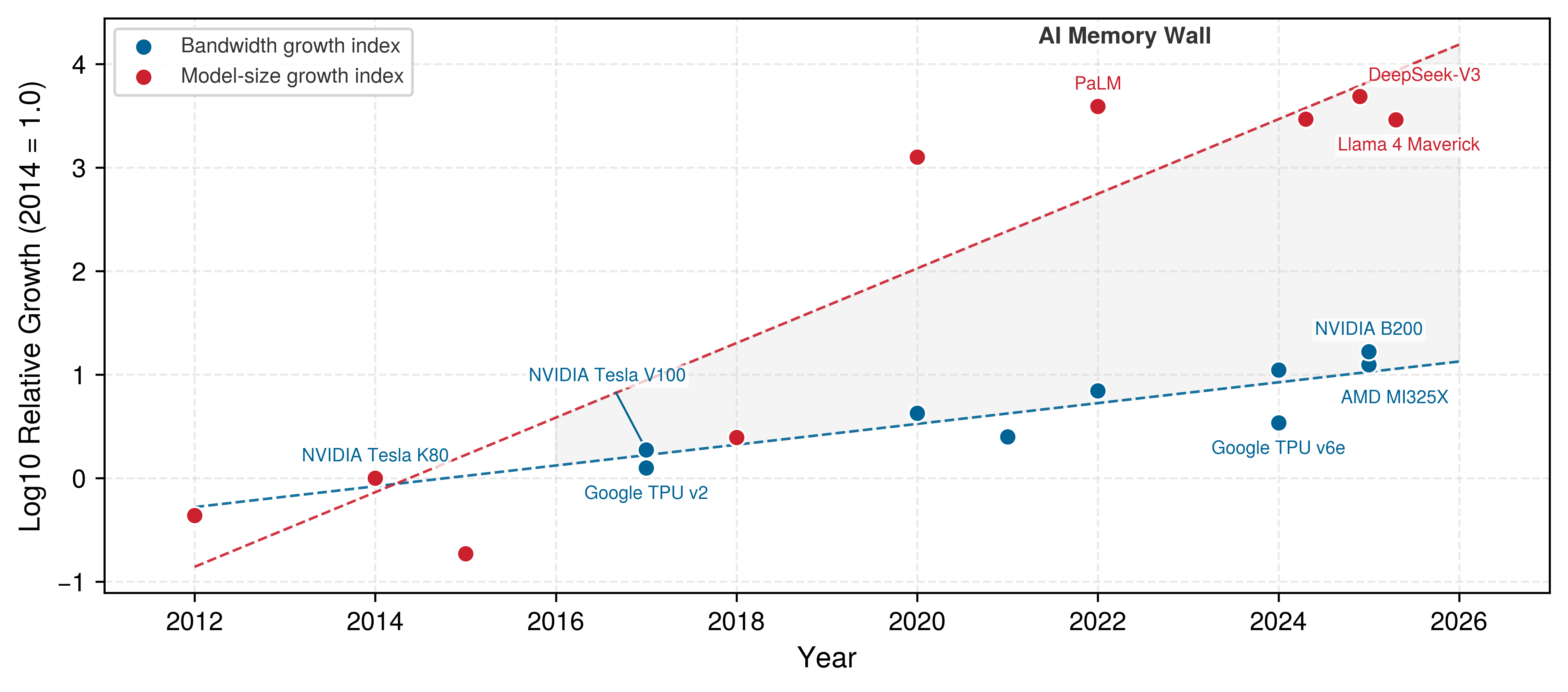
The generations in figure 9 come from one vendor, but the divergence is industry-wide. Figure 10 tracks the best memory bandwidth and the best dense FP16/BF16 tensor throughput among 52 accelerators from every major vendor released since 2017 (Epoch AI 2026). Measured from TPU v2, the best compute rate grew about 55× while the best bandwidth grew about 13×, so the ridge point of the leading devices rose several-fold; the ratio is larger than the NVIDIA-only one above because TPU v2’s 16-bit baseline was low. Since early 2025 the best bandwidth has held near 8 TB/s, and the best dense FP16 rate has leveled as well, because new devices put their added arithmetic into FP8 and FP4 paths rather than 16-bit ones. For a kernel whose reuse stays fixed, this rising ridge shows up as a ceiling on achievable utilization that falls with each generation.
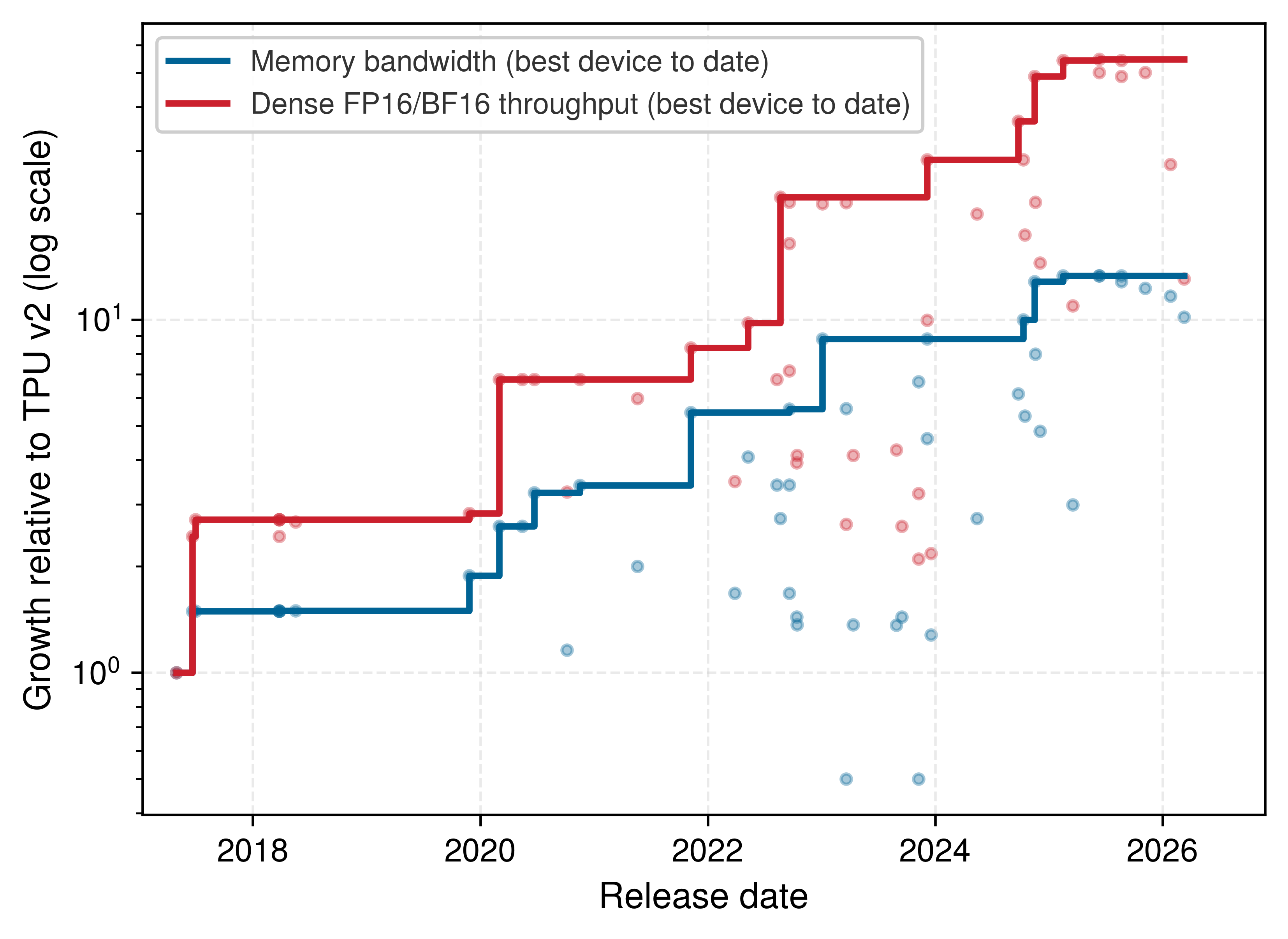
Epoch AI. 2026. Machine Learning Hardware.
Napkin Math 11.3: The utilization gap
Problem: Why is it harder to get 100 percent utilization on an H100 than a V100?
Metric: The ridge point \(\RooflineRidgePoint = \PeakRate / \Bandwidth\) (FLOP/byte), the number of operations the hardware must perform for every byte loaded to keep its compute units busy.
Result: The intensity needed to reach the tensor peak has increased. Under this simple HBM roofline, a kernel with \(\ArithmeticIntensity\) = 200 FLOP/byte lies above the A100 ridge but below the H100 ridge. If its intensity and implementation remain unchanged, its idealized gain is then closer to the 1.6× bandwidth ratio than the 3.2× peak-compute ratio.
Systems insight: Fusion is valuable for low-intensity chains because it can remove intermediate round-trips; it is not automatically the best optimization for every kernel.
Operations such as depthwise convolution, embedding lookup, LayerNorm, and softmax serve as low-intensity reference points that commonly fall below the HBM ridge on compute-dense accelerators under the stated traffic models. Table 7 maps common neural network operations to their representative roofline regimes and to the lighthouse workload that exercises each. Classification depends on the implementation, memory interface, and target path; profiling distinguishes a bandwidth ceiling from latency, limited parallelism, or other execution constraints.
| Operation | Arithmetic Intensity | Classification | Lighthouse example |
|---|---|---|---|
| Conv2D (Dense) | 50–200 FLOP/byte | Straddles ridge; high-reuse cases compute-bound | ResNet-50 |
| Dense MatMul (large batch, well-tiled) | ~150–1,000+ FLOP/byte | Compute-bound once above the target’s ridge | GPT-2 (batched projections) |
| Depthwise conv | 10–20 FLOP/byte | Below modeled HBM ridge | MobileNet |
| Attention Softmax | Convention-dependent | Below modeled HBM ridge | GPT-2 (Generation) |
| LayerNorm | 1–2 FLOP/byte | Below modeled HBM ridge | GPT-2/Llama |
| Embedding lookup | \(<1\) FLOP/byte | Below modeled HBM ridge | DLRM |
Napkin Math 11.4: Transformer layer analysis
For one GPT-2 XL layer during prefill, with hidden dimension \(\HiddenDimension\) = 1600, batch size \(\BatchSize\) = 8, sequence length \(\SequenceLength\) = 1024, and \(\AttentionHeadCount\) = 25 attention heads:
Attention QKV projection:
- FLOPs: 2 \(\times\) 3 \(\times\) 8 \(\times\) 1024 \(\times\) 1600 \(\times\) 1600 = 125.8 GFLOP
- Bytes: (input + weights + output) = (8 \(\times\) 1024 \(\times\) 1600 + 3 \(\times\) 1600 \(\times\) 1600 + 8 \(\times\) 1024 \(\times\) 1600 \(\times\) 3) \(\times\) 2 ≈ 120.2 MB
- \(\ArithmeticIntensity\) = 125.8 GFLOP / 120.2 MB = 1046.7 FLOP/byte, which is compute bound on the H100 (above the 295.2 FLOP/byte ridge point)
Softmax:
- FLOPs: 8 \(\times\) 25 \(\times\) 1024 \(\times\) 1024 \(\times\) 3 ≈ 629.1 MFLOP (exp, sum, div)
- Bytes: 8 \(\times\) 25 \(\times\) 1024 \(\times\) 1024 \(\times 2 \times 2\) = 838.9 MB
- \(\ArithmeticIntensity\) = 629.1 MFLOP / 838.9 MB = 0.75 FLOP/byte under this simple operation count, placing it below the reference tensor-path HBM ridge. Counting exponentials and division as multiple operations raises the numerical intensity, but those instructions use different execution units. The relevant vector, reduction, and special-function ceilings, together with profiling, determine whether bandwidth actually binds.
Systems insight: This analysis explains why FlashAttention focuses on reducing memory traffic in attention rather than reducing FLOPs.
The roofline supplies an initial resource bound; profiling determines which physical subsystem limits the kernel. When a kernel approaches its relevant off-chip bandwidth ceiling, optimization should focus on conserving memory traffic: fusing adjacent operators keeps intermediate activations in on-chip registers or shared memory (SRAM), lower-precision numeric formats reduce the physical byte count of memory transfers, and algorithmic refactorings like FlashAttention restructure access patterns to compute within SRAM tiles. When a kernel approaches the compute ceiling of its actual execution path, high data reuse keeps execution units supplied and off-chip bandwidth is no longer the binding resource. Performance here depends on saturating arithmetic execution pipelines: structuring matrix tiles to sustain Tensor Core throughput, hiding instruction latencies through software pipelining, and scaling batch sizes to distribute work across all available streaming multiprocessors.
↪ How a benchmark determines where a workload actually sits against its roofline ceiling is developed in System benchmarks.
11.6.3 Memory bandwidth bounds
When a kernel’s arithmetic intensity falls below the ridge point, adding more Tensor Cores cannot speed it up because off-chip memory bandwidth cannot deliver operands fast enough to sustain the target compute rate \(\TargetComputeRate\) (FLOP/s). For a workload with arithmetic intensity \(\ArithmeticIntensity\) (FLOP/byte), keeping the compute units fed at rate \(\TargetComputeRate\) requires the memory subsystem to transfer data at the rate defined by equation 3: \[\RequiredMemoryBandwidth = \frac{\TargetComputeRate}{\ArithmeticIntensity} \text{ bytes/s} \tag{3}\]
When this required bandwidth exceeds the hardware’s peak memory bandwidth \(\Bandwidth\), memory transfers cap attainable throughput according to equation 4: \[\AttainableComputeRate = \Bandwidth \times \ArithmeticIntensity \tag{4}\]
Evaluating an operation against its execution path’s ridge point identifies the lower modeled ceiling. Extensive data reuse can raise arithmetic intensity above that ridge, making compute the tighter bound; profiling must establish whether execution approaches it. ResNet-50’s stage-3 \(3{\times}3\) convolution demonstrates this behavior.
Napkin Math 11.5: Convolutional layer analysis
Consider the \(3{\times}3\) convolution in a stage-3 bottleneck block of ResNet-50, with input shape (batch = 32, channels = 128, height = 28, width = 28) and 128 output channels, on an H100 at FP16:
Computational requirements:
- Output size: \(32 \times 128 \times 28 \times 28\) = 3.2M elements
- FLOPs per output: \(128 \times 3 \times 3 \times 2\) = 2,304 (multiply-add)
- Total FLOPs: 3.2M \(\times\) 2,304 = 7.4 GFLOP
Memory traffic analysis:
- Input: \(32 \times 128 \times 28 \times 28 \times 2\) = 6.4 MB (FP16)
- Weights: \(128 \times 128 \times 3 \times 3 \times 2\) ≈ 0.3 MB (FP16)
- Output: \(32 \times 128 \times 28 \times 28 \times 2\) = 6.4 MB (FP16)
- Total: 13.1 MB
Arithmetic intensity: \(\ArithmeticIntensity\) = 7.4 GFLOP / 13.1 MB = 563.1 FLOP/byte
Systems insight: This is well above the H100’s FP16 ridge point of 295.2 FLOP/byte, so the simple roofline model places the operation in the compute-limited region. The dense FP16 tensor peak of ~989 TFLOP/s is therefore the ceiling, but realized performance still depends on tiling, occupancy, instruction mix, and library efficiency.
The convolutional layer’s high arithmetic intensity arises from spatial weight reuse: the same \(3{\times}3\) kernel is applied across every spatial location in the feature map, amortizing the cost of loading weights from off-chip memory across millions of multiply-accumulate operations. Keeping active tiles in registers and shared memory reduces repeated off-chip transfers, making high arithmetic throughput possible. Whether a particular kernel then saturates the Tensor Cores depends on tiling, occupancy, and instruction mix, which the roofline does not model. Moreover, the FP16 analysis is only half of the chapter’s workload, because the profile Model Compression ended on runs ResNet-50 in INT8; quantization changes both sides of the roofline at once, and the two changes need not cancel.
Napkin Math 11.6: When INT8 moves a layer below the ridge
Problem: The H100’s INT8 tensor path offers about 2× the operations per second of its FP16 path from the same 3.35 TB/s of memory bandwidth. Which ResNet-50 layers stay compute bound when the model moves from FP16 to INT8?
The two ridges: The ridge rises from 295.2 FLOP/byte at FP16 to 590.7 FLOP/byte at INT8. A layer keeps its position relative to the ridge only if every byte it moves halves along with the operand width.
Three layers at batch 32 (operations per byte, one read of input and weights and one write of the output):
- Stage-3 \(3{\times}3\) convolution (the layer of notebook 11.5): 563 at FP16, above the FP16 ridge. With INT8 activations it reaches 1,126, above the INT8 ridge. If its activations stay FP16 between layers, as when the kernel reads and writes 16-bit tensors for FP16 neighbors, its intensity stays near 569, below the INT8 ridge.
- Stage-2 \(3{\times}3\) convolution (\(56{\times}56\) positions, 64 channels in and out): 287 at FP16 and 574 at INT8, just below the ridge in both precisions.
- Stage-2 \(1{\times}1\) expansion (\(56{\times}56\) positions, 64 channels in and 256 out): 51 at FP16 and 102 at INT8, far below the ridge in both.
Systems insight: INT8 raises the arithmetic ceiling but leaves the bandwidth ceiling where it was, so the layers that were already bandwidth bound gain only the halved bytes, and a compute-bound layer whose activations stay wide crosses below the new ridge. The INT8 speedup of Model Compression’s profile therefore depends on whether activations travel at INT8 between layers, a decision made by the compiler and runtime (section 11.8), not by the quantized weights alone.
Not all neural network layers reuse data so heavily. Fully connected (dense) layers, such as ResNet-50’s classification head, feed-forward networks, and linear projections in transformer attention blocks, lack spatial dimensions. When evaluated at small batch sizes, their arithmetic intensity drops substantially, shifting execution into the bandwidth-bound regime:
Napkin Math 11.7: Dense layer analysis
Consider ResNet-50’s final fully connected layer, which maps 2,048 pooled features to 1,000 class scores for a batch of 32 images on the same H100:
Computational requirements:
- Matrix multiply: \((32 \times 2048) \times (2048 \times 1000)\)
- Total FLOPs: \(2 \times 32 \times 2048 \times 1000\) = 131.1 MFLOP
Memory traffic analysis:
- Input: \(32 \times 2048 \times 2\) = 131.1 KB (FP16)
- Weights: \(2048 \times 1000 \times 2\) = 4.1 MB (FP16)
- Output: \(32 \times 1000 \times 2\) = 64 KB (FP16)
- Total: 4.3 MB
Arithmetic intensity: \(\ArithmeticIntensity\) = 131.1 MFLOP / 4.3 MB = 30.5 FLOP/byte
This intensity sits below the H100’s ridge point of 295.2 FLOP/byte, making this operation memory bound under the stated traffic model. Attainable performance: \(\AttainableComputeRate\) = 3,350 GB/s \(\times\) 30.5 FLOP/byte = 102.3 TFLOP/s
Systems insight: Attainable throughput is only 10.3 percent of peak compute capability, so at batch 32 the memory wall caps this layer long before the Tensor Cores do.
The dense layer’s lower arithmetic intensity stems from limited parameter reuse. While a convolutional kernel is reused across every spatial location in an activation map, a dense weight matrix is reused only across the batch dimension. At a batch size of 32, each fetched weight contributes to 32 sample products in this operation. When the weights stream from HBM on each invocation, as modeled, the bandwidth ceiling caps throughput at 10.3 percent of peak compute capacity. The fraction is a bound rather than a measured stall count, and a layer whose weights stay cached between invocations would do better. The same arithmetic explains why transformer inference at low batch sizes is governed by memory bandwidth rather than arithmetic capability, a regime the throughput-ceiling notebook below quantifies for GPT-2.
While small-batch matrix multiplications suffer from restricted parameter reuse, elementwise and reduction operators represent an even more acute memory bottleneck. Operations such as layer normalization, activation functions, and residual additions perform only a few arithmetic operations per element loaded from memory, driving arithmetic intensity to its physical floor:
Napkin Math 11.8: LayerNorm analysis
LayerNorm over one GPT-2 XL layer’s activations, with input shape (batch = 8, sequence = 1024, hidden = 1600):
Computational requirements:
- Elements: \(8 \times 1024 \times 1600\) = 13.1M
- Approximate operations per element: mean reduction (1 ADD), variance (2 ADD, 1 MUL), normalization and affine transform (2 ADD, 2 MUL) ≈ 8; reciprocal-square-root overhead is amortized across each hidden vector
- Total FLOPs: 13.1M \(\times\) 8 = 104.9 MFLOP
Memory traffic:
- Input: 13.1M \(\times\) 2 = 26.2 MB
- Parameters (scale, bias): \(1600 \times 2 \times 2\) = 6.4 KB (negligible)
- Output: 13.1M \(\times\) 2 = 26.2 MB
- Total: 52.4 MB
Arithmetic intensity: \(\ArithmeticIntensity\) = 104.9 MFLOP / 52.4 MB = 2.0 FLOP/byte
This arithmetic intensity sits severely below the H100 ridge point (148× below). The HBM performance upper bound is: \(\AttainableComputeRate\) = 3,350 GB/s \(\times\) 2.0 FLOP/byte = 6.7 TFLOP/s
Systems insight: The simple HBM roofline bounds this standalone LayerNorm at about 0.7 percent of the H100’s tensor peak. That tensor peak is a reference, not the throughput available to LayerNorm’s vector and reduction instructions. Actual latency also depends on their execution ceilings, fusion, launch overhead, and which memory level supplies the data.
Standalone normalization performs minimal arithmetic relative to the memory traffic it generates, as the LayerNorm analysis demonstrates. Under the modeled unfused HBM read/write boundary, the implementation performs approximately 2 FLOP/byte, giving a low bandwidth ceiling relative to the tensor peak. Reaching that ceiling still requires enough parallel work and an efficient reduction. Cache residency changes the physical HBM byte count and can shift the relevant bound to another memory interface. In the D·A·M framework, when the machine constraint is a memory bandwidth wall, the algorithmic response is kernel fusion, which collapses adjacent projections, bias additions, normalization, and activations into one kernel so that intermediate values stay in registers or SRAM. Fusion pays off when the grouping preserves numerical behavior and fits the local register and SRAM budget, and profiling confirms that the saved traffic outweighs any loss of occupancy.
11.6.4 Optimization by intensity regime
Tuning thread-block occupancy on a bandwidth-bound LayerNorm kernel wastes engineering effort for zero speedup, just as fusing two already compute-bound matrix multiplications cannot raise throughput past the Tensor Core ceiling. The roofline’s intensity regimes (table 8) match each bottleneck to the lever that can move it.
| Intensity regime | Typical operations | Optimization priority | Common techniques | Expected impact |
|---|---|---|---|---|
| Above the target path’s ridge | Large convolutions | Maximize compute utilization. | Tensor Cores, thread-block tuning, and high occupancy. | Raises sustained compute utilization when the kernel already clears the ridge. |
| Near the target path’s ridge | Medium-sized dense layers | Balance compute and memory optimization. | Larger batches, register tiling, and fusion with adjacent operations. | Can move the binding bottleneck between memory and compute. |
| Below the target path’s ridge | Small dense layers and element-wise operations | Reduce memory traffic. | Aggressive kernel fusion, reduced precision (FP16 → INT8), and algorithmic changes. | Reduces external-memory traffic when fusion or layout changes are legal. |
| Low-intensity operator chains | Normalization layers and activation functions | Eliminate memory round-trips. | Fuse with adjacent operations and use in-place computation where legal. | Removes intermediate round-trips when adjacent operations can be fused. |
For low-intensity operations, kernel fusion is often the decisive optimization: LayerNorm combined with the Gaussian Error Linear Unit (GELU), for example, can become a single fused kernel. One of the most accessible levers for moving an operation up and right on the roofline is batching.
Napkin Math 11.9: Batch size and arithmetic intensity
Increasing batch size improves arithmetic intensity for matrix operations by amortizing weight loading. Equation 5 formalizes this relationship for an idealized FP16/BF16 dense layer \((\BatchSize{\times}\LayerInputWidth){\times}(\LayerInputWidth{\times}\LayerOutputWidth)\), counting one read each of the input and weights and one write of the output, where \(\BatchSize\) is batch size and \(\LayerInputWidth\) and \(\LayerOutputWidth\) are the layer’s input and output widths: \[\ArithmeticIntensity = \frac{2\BatchSize\LayerInputWidth\LayerOutputWidth}{2\BatchSize\LayerInputWidth + 2\LayerInputWidth\LayerOutputWidth + 2\BatchSize\LayerOutputWidth} \approx \frac{2\BatchSize\LayerInputWidth\LayerOutputWidth}{2\LayerInputWidth\LayerOutputWidth} = \BatchSize\quad (\text{when } 2\LayerInputWidth\LayerOutputWidth \gg 2\BatchSize(\LayerInputWidth+\LayerOutputWidth)) \tag{5}\]
Example: Dense layer with \(\LayerInputWidth = \LayerOutputWidth\) = 2048 (FP16)
- Batch = 1: \(\ArithmeticIntensity\) ≈ 1 FLOP/byte (memory bound)
- Batch = 32: \(\ArithmeticIntensity\) ≈ 31 FLOP/byte (memory bound)
- Batch = 512: \(\ArithmeticIntensity\) ≈ 341.3 FLOP/byte (compute bound on the H100)
Systems insight: This explains why batching can produce large throughput improvements in production inference systems, as MLPerf Inference, the standardized benchmark suite, demonstrates by separating bulk-throughput runs from latency-constrained serving runs (Reddi et al. 2019).
Reddi, Vijay Janapa, Christine Cheng, David Kanter, Peter Mattson, Guenther Schmuelling, Carole-Jean Wu, Brian Anderson, et al. 2019. “MLPerf Inference Benchmark.” 2020 ACM/IEEE 47th Annual International Symposium on Computer Architecture (ISCA), 446–59. https://doi.org/10.1109/isca45697.2020.00045.
↪ The MLPerf Inference execution scenarios that separate throughput runs from latency-constrained runs are developed in MLPerf execution scenarios.
The batch size analysis reveals why inference serving systems are designed around batching: it changes the arithmetic intensity regime of bandwidth-bound workloads. However, batching introduces latency trade-offs, since requests must wait in a queue until a batch forms. This tension between throughput (favoring large batches) and latency (favoring small batches) is a central challenge in ML serving systems, explored in depth in Dynamic batching latency-throughput trade-offs. When service latency limits batching, batch-1 or small-batch LLM decode often retains low weight reuse and low arithmetic intensity, and the next worked model quantifies that particular regime rather than treating all LLM inference as identical.
Napkin Math 11.10: The throughput ceiling
Problem: A batch-1 GPT-2 calculation makes this bandwidth ceiling concrete: what is the maximum possible utilization of an NVIDIA H100 when running GPT-2 inference (batch size 1)?
The hardware constraints (the denominators)
Peak compute: 989 TFLOP/s (FP16 Tensor Core).
Peak bandwidth: 3.35 TB/s (HBM3).
Ridge point \((\PeakRate/\Bandwidth)\): 989 TFLOP/s / 3.35 TB/s = 295.2 FLOP/byte (for FP16 Tensor Core).
Interpretation: Saturating this chip at FP16 precision requires 295.2 FLOP/byte operations for every byte loaded. The ridge point varies by precision: FP32 operations (67 TFLOP/s peak) have a ridge point of only ~20 FLOP/byte.
The workload characteristics (the numerator)
- Model: GPT-2 XL (1.5 billion parameters).
- Operation: Autoregressive generation (1 token at a time).
- Data movement: Must load all weights (3 GB @ FP16) for every token.
- Compute: Vector-Matrix multiplication. Two FLOPs per parameter, \(2\Parameters\) ≈ 3 GFLOP.
- Arithmetic intensity: 3 GFLOP / 3 GB = 1 FLOP/byte
The prediction (iron law)
Since the modeled intensity \(\ArithmeticIntensity\) (1) \(\ll\) the ridge point \(\RooflineRidgePoint\) (295.2 FLOP/byte), batch-1 decode is bandwidth bound.
- Maximum throughput: 1 FLOP/byte \(\times\) 3.35 TB/s = 3.4 TFLOP/s.
- Utilization ceiling: 3.4 TFLOP/s (Bound) / 989 TFLOP/s (Peak) ≈ \(0.3\%\)
Systems insight: Without batching, a ~$25,000 accelerator cannot exceed 0.3 percent of its compute peak in this weight-streaming decode scenario. Batching and weight quantization address that gap; key-value caching instead avoids recomputing prior attention states. The ceiling also assumes that the decode step is launched as a captured graph (Graph capture and JIT compilation); executed one eager kernel at a time, launch overhead rather than weight streaming would set the floor.
Placed on one roofline, the layers and the decode step analyzed above fall on either side of two ridges, and only the stage-3 \(3{\times}3\) convolution reaches a flat ceiling (figure 11). Through this derivation, the roofline model provides a diagnostic framework for identifying whether operations are compute bound or memory bound. Knowing that batch-1 decode is bandwidth bound at a ceiling of 0.3 percent of peak is only the first step; the next challenge is translating this diagnosis into efficient execution plans that exploit accelerator architectures.
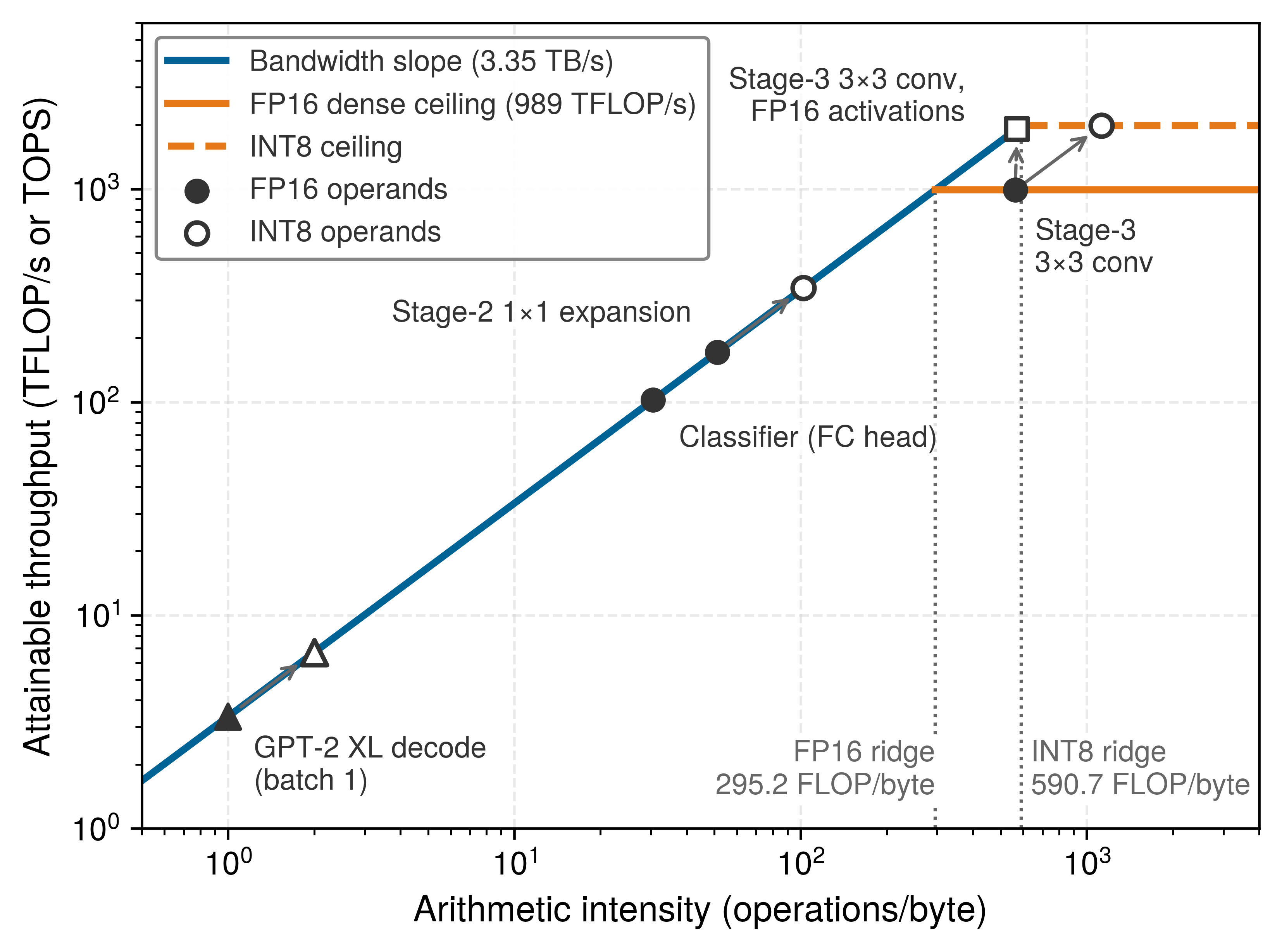
Checkpoint 11.3: The machine and its ceilings
The first half of the chapter has assembled the accelerator and its two ceilings. Before turning to how software reaches them, check that you can work from the anatomy to a bound.
Compute units
Memory systems
Performance bounds
Self-Check: Question
An accelerator delivers \(R_{\text{peak}} = 1{,}000\text{ TFLOP/s}\) (\(10^{15}\text{ FLOP/s}\)) in FP16 and has a High-Bandwidth Memory (HBM) subsystem delivering \(\text{BW} = 2.0\text{ TB/s}\) (\(2\times 10^{12}\text{ bytes/s}\)). What is the hardware balance point (ridge point \(I_{\text{ridge}}\)) of this system?
- \(50\text{ FLOP/byte}\)
- \(200\text{ FLOP/byte}\)
- \(500\text{ FLOP/byte}\)
- \(2{,}000\text{ FLOP/byte}\)
A developer runs a LayerNorm kernel on an accelerator with \(R_{\text{peak}} = 312\text{ TFLOP/s}\) and \(\text{BW} = 1.5\text{ TB/s}\) (\(I_{\text{ridge}} = 208\text{ FLOP/byte}\)). The LayerNorm has an arithmetic intensity of \(I = 4\text{ FLOP/byte}\). What is the maximum attainable performance under this simple roofline model, and what modeled ceiling is lower?
- \(6.0\text{ TFLOP/s}\), the bandwidth ceiling
- \(312\text{ TFLOP/s}\), the compute ceiling
- \(78\text{ TFLOP/s}\), the warp-scheduler ceiling
- \(1.5\text{ TFLOP/s}\), the PCIe ceiling
Why has the hardware ridge point (\(I_{\text{ridge}}\)) increased across successive GPU generations, and what pressure does this trend place on compiler and kernel developers?
True or False: When a kernel operates in the memory-bound regime of the Roofline model (\(I < I_{\text{ridge}}\)), doubling the accelerator’s peak tensor compute capability (\(R_{\text{peak}}\)) without changing memory bandwidth will double the kernel’s execution speed.
In the Roofline model, the transition point on the horizontal axis where the memory-bandwidth ceiling intersects the peak-compute ceiling is known as the hardware ____ point.
An engineer profiles a transformer inference workload and discovers that the attention Softmax kernel is heavily memory bandwidth bound. Which of the following optimization techniques directly targets intermediate-memory traffic in this kernel?
- Upgrading host CPU RAM to DDR5 to decrease kernel enqueue latency
- Fusing the scale, mask, and Softmax stages into a single kernel to keep intermediates in registers or SRAM when resources allow
- Increasing the clock frequency of the GPU Tensor Cores by \(15\%\)
- Disabling warp scheduler out-of-order instruction issue
11.7 Hardware Mapping
Consider one of ResNet-50’s \(3{\times}3\) convolutions running on an accelerator tile. The mathematical operation is fixed, but the execution plan is not. One schedule can keep a filter in local registers while many output pixels stream past it; another can advance pixel by pixel and reload the same filter values repeatedly from a slower memory tier. Both schedules compute the same tensor. Only one turns the reuse in the convolution into real bandwidth savings.
Definition 11.4: Mapping in AI acceleration
Mapping in AI acceleration is the accelerator-compiler process of binding the logical computation graph to the physical hardware topology by deciding which operations execute on which processing elements, which data resides in which memory tier, and in what temporal order.
- Significance: Within the D·A·M taxonomy, mapping is a machine-axis decision that helps determine how closely an operation approaches the roofline bound \(\min(\PeakRate,\; \Bandwidth \times \ArithmeticIntensity)\). A poor tiling choice that forces unnecessary DRAM accesses can reduce effective arithmetic intensity enough to move a nominally compute-bound operation into the bandwidth-bound regime.
- Distinction: Traditional compilation often emphasizes instruction selection, register allocation, and scheduling for general-purpose processors. Accelerator mapping gives equal prominence to spatial placement and explicit data movement across a dataflow architecture. The reason is physical: as quantified by the storage-tier energy ladder in figure 4, an off-chip DRAM access costs about 173× the energy of an FP32 multiply, making operand placement as critical to efficiency as the execution unit that evaluates it.
- Common pitfall: A frequent misconception is that mapping is automatically handled by frameworks. For general GPU workloads, compilers such as Accelerated Linear Algebra (XLA) can find strong mappings for common kernels; for specialized accelerators (systolic arrays, custom ASICs), compiler-generated mappings may still lag hand-tuned schedules because the compiler’s search space is limited by the time budget at compilation.
The convolution example exposes the three decisions that recur throughout accelerator compilation. Placement assigns the multiply-accumulate work to processing elements so parallelism does not turn into idle time or interconnect congestion. Allocation keeps weights, activations, and partial sums in the memory tier where their next use will occur, rather than letting reuse spill back to DRAM. Scheduling orders loops and kernels so the chosen placement and allocation remain valid over time. A poor choice in any one dimension can collapse a high-arithmetic-intensity operation back into a bandwidth-bound execution. In practice, these choices are too coupled for developers to manage by hand at model scale, which is why systems such as XLA, TVM, and TensorRT lower high-level models and search or select execution plans within their compile-time and hardware budgets. Section 11.8 examines that compiler support in detail.
11.7.1 Placement and allocation
Translating a model’s computational graph into efficient hardware execution requires solving two tightly coupled problems. Computation placement determines which operations run on which processing elements, balancing parallelism against communication costs. Memory allocation determines where data resides within the memory hierarchy, trading capacity against access latency. These two decisions interact: placing operations on distant processing elements increases the memory bandwidth required to shuttle data between them, while allocating data to fast but small on-chip memory limits which operations can execute concurrently. Getting either wrong leaves thousands of processing elements idle or starved for data.
Computation placement
Computation placement is the process of assigning operations to an accelerator’s processing elements (PEs) to expose parallelism, limit idle time, and reduce unnecessary data movement. Modern accelerators contain many such resources: the NVIDIA H100 has more than 16,000 CUDA cores and more than 500 Tensor Cores (Choquette 2023), TPUs organize thousands of multiply-accumulate units into systolic arrays (Jouppi et al. 2017), and wafer-scale processors such as Cerebras’ CS-2 integrate more than 850,000 cores (Systems 2021). At these scales, placement inefficiencies become measurable because idle cores and redundant transfers waste both time and energy.
The difficulty of placement depends on workload regularity. Convolutional networks and dense transformer operations possess regular access patterns that tile predictably, though transformer architectures mix operations with distinct tensor shapes and reuse profiles. Graph neural networks (GNNs) present greater difficulty: sparse, input-dependent neighborhood aggregations introduce load imbalance and non-uniform communication across processing elements. Table 9 summarizes these core placement challenges and their operational impact.
| Challenge | Impact on execution | Key Considerations for Placement |
|---|---|---|
| Workload imbalance | Some processing elements finish early while others remain overloaded, leading to idle compute resources. | Distribute operations evenly to prevent stalls and ensure full utilization of PEs. |
| Irregular computation patterns | Sparse graphs, routing, and variable shapes can create nonuniform work that complicates static placement. | Use adaptive placement when workload characteristics vary at run time. |
| Excessive data movement | Frequent memory transfers introduce latency and increase power consumption. | Keep frequently used data close to the compute units and minimize off-chip memory accesses. |
| Limited interconnect bandwidth | Poorly placed operations can create congestion, slowing data movement between PEs. | Optimize spatial and temporal placement to reduce communication overhead. |
| Model-specific execution needs | CNNs, transformers, and GNNs require different execution patterns, making a single placement strategy ineffective. | Tailor placement strategies to match the computational structure of each model type. |
Static spatial mappings suffice for regular dense operations whose shapes and loop bounds are known ahead of time. Workloads with dynamic shapes, sparsity, or mixture-of-experts routing instead require runtime scheduling to balance execution across processing elements. Yet even an optimal computation placement stalls if the required operands are not staged in time: compute units can execute only as fast as operands arrive from the memory hierarchy.
Memory allocation
While computation placement determines where operations execute, memory allocation defines where data resides and how it flows through the hierarchy. The goal is to keep reused data near the processing elements without exceeding faster-tier capacity. GPUs expose global memory, shared memory, caches, and registers that kernels coordinate through tiling (NVIDIA Corporation 2020a). TPUs use on-chip SRAM buffers to stage the activations that flow horizontally through the 2D systolic-array dataflow (Jouppi et al. 2017) of figure 5, with partial sums flowing vertically, while wafer-scale processors partition memory and computation to control interconnect traffic (Systems 2021). General-purpose processors and accelerators both use memory hierarchies, but many accelerators expose more placement decisions to compilers and kernels. When allocation fails to exploit locality, processing elements stall waiting for operands, driving down utilization and dissipating energy across the memory bus.
Systems, Cerebras. 2021. “Wafer-Scale Deep Learning Acceleration with the Cerebras CS-2.” Cerebras Technical Paper 2021.
The severity of these penalties varies by workload. Convolutional networks rely on structured, localized access patterns and benefit from well-defined memory layouts that support predictable reuse (Chen et al. 2016). Transformers require access to large parameter sets and intermediate activations, making them sensitive to capacity and bandwidth. Graph neural networks add irregular sparse structures that complicate allocation and prefetching.
Capacity is only the first allocation test. A tensor can fit in accelerator memory yet still dominate execution if each kernel rereads it from a distant tier; conversely, tiling can keep a larger working set efficient by preserving reuse locally. The allocation diagnostic is therefore traffic, not capacity alone: compilers must track how frequently values cross each memory boundary and keep high-reuse tensors in the fastest feasible tier. Systems combine static memory plans for known shapes with dynamic buffer management when shapes vary, while device capacity limits which models fit without partitioning or offload. Table 10 summarizes these allocation challenges across the hierarchy.
| Challenge | Impact on Execution | Key Considerations for Allocation |
|---|---|---|
| High memory latency | Slow data access delays execution and reduces throughput. | Prioritize placing frequently accessed data in faster memory locations. |
| Limited on-chip storage | Small local memory constrains the amount of data available near compute units. | Allocate storage efficiently to maximize data availability without exceeding hardware limits. |
| High off-chip bandwidth demand | Frequent access to external memory increases delays and power consumption. | Reduce unnecessary memory transfers by carefully managing when and how data is moved. |
| Irregular memory access patterns | Some models require accessing data unpredictably, leading to inefficient memory usage. | Organize memory layout to align with access patterns and minimize unnecessary data movement. |
| Model-specific memory needs | Different models require different allocation strategies to optimize performance. | Tailor allocation decisions based on the structure and execution characteristics of the workload. |
11.7.2 Combinatorial complexity
The convolution that opened this section illustrates why hardware mapping becomes a combinatorial search problem. Keeping a filter resident in local storage improves reuse only if the assigned processing elements have sufficient storage and if the loop schedule revisits that filter before eviction. Similarly, parallelizing across more processing elements improves throughput only until synchronization overhead and interconnect contention erode the benefit. Because changing one decision alters the feasible and efficient choices for the others, compilers must evaluate placement, allocation, and scheduling jointly rather than independently. Table 11 summarizes these recurring trade-offs across the execution stack.
| Dimension | Placement considerations | Allocation and Scheduling Considerations |
|---|---|---|
| Computational granularity | Fine-grained placement enables greater parallelism but increases synchronization overhead. | Coarse-grained scheduling reduces synchronization overhead but may limit flexibility. |
| Spatial vs. Temporal Mapping | Spatial placement enhances parallel execution but can lead to resource contention and memory congestion. | Temporal scheduling balances resource sharing but may reduce overall throughput. |
| Memory and Data Locality | Placing data closer to compute units minimizes latency but may reduce overall memory availability. | Allocating data across multiple memory levels increases capacity but introduces higher access costs. |
| Communication and synchronization | Co-locating compute units reduces communication latency but may introduce contention. | Scheduling synchronization mechanisms mitigates stalls but can introduce additional overhead. |
| Dataflow and Execution Ordering | Static placement simplifies execution but limits adaptability to workload variations. | Dynamic scheduling improves adaptability but adds scheduling complexity. |
Counting the search space
Evaluating these trade-offs requires navigating an unconstrained search space governed by three structural decisions: loop execution order, spatial parallelization across processing elements, and memory placement across the hierarchy. Counting each dimension on its own shows why exhaustive search is impractical.
Machine learning workloads are expressed as nested loops over tensor dimensions, and the loop execution order dictates which tensor elements remain resident in registers or SRAM between iterations. Ignoring dependences and equivalent orderings, the number of ways to arrange \(\LoopNestDepth\) loops has the toy upper bound: \[ \LoopOrderCount= \LoopNestDepth! \] A convolutional layer with seven loop dimensions already has \(7! = 5{,}040\) possible execution orders. If each memory level could choose an ordering independently, the toy upper bound would expand as: \[ (\LoopNestDepth!)^{\MemoryHierarchyLevelCount} \] where \(\MemoryHierarchyLevelCount\) is the number of memory hierarchy levels. A suboptimal ordering evicts values prematurely and multiplies DRAM traffic, whereas an optimized ordering maximizes reuse in local SRAM and caches (Sze et al. 2017).
Parallelization multiplies the count again. Parallelizing outer independent loops (such as batch or output feature channels) lets each core execute without interconnect traffic, whereas parallelizing an inner reduction loop requires cross-core synchronization and collective communication. Before legality and capacity constraints are applied, the number of ordered ways to select loops for parallel execution has the upper bound: \[ \LoopParallelizationChoiceCount= \frac{\LoopNestDepth!}{(\LoopNestDepth-\ParallelLoopCount)!} \] where \(\ParallelLoopCount\) is the number of loops selected for parallel execution; three of six loops already give \(6!/3! = 120\) candidates, each with different demands on synchronization, interconnect bandwidth, and PE utilization. Memory placement is the third dimension, and physical capacity bounds it. Because an off-chip DRAM fetch costs roughly 128\(\times\) more energy than a read from an 8 KB SRAM array (figure 4), where each tensor resides directly dictates the achieved arithmetic intensity, yet an operand tile can remain in on-chip SRAM only if its working set fits the allocated buffer. Larger resident tiles raise reuse but consume scarce capacity and register pressure, potentially reducing thread concurrency or forcing spills to slower tiers.
Per memory level, from the section’s separate toy examples: \(4^5 = 1{,}024\) placements, \(7! = 5{,}040\) orders, \(6!/3! = 120\) parallelizations. The product is raised to the number of levels, so three levels give \(4^{15}\) placements alone.
These structural choices (loop ordering, spatial parallelization across processing elements, tile sizing, and memory placement) are deeply coupled. Choosing an output-stationary schedule, for example, pins accumulators in local registers and dictates which loops can be mapped spatially across processing elements without requiring inter-core reduction networks. Conversely, parallelizing across more execution units reduces the per-core SRAM budget available for operand staging, forcing smaller tile dimensions and increasing off-chip memory traffic.
While the unconstrained Cartesian product of these decisions suggests a massive combinatorial space, hardware capacity limits, data dependencies, and symmetry prune the vast majority of candidates as either physically illegal or strictly dominated. Exhaustive search across arbitrary loop permutations and placement choices is therefore both unnecessary and intractable. Production compilers and kernel developers manage this complexity by structuring their search around a small family of canonical dataflow patterns, spatial and temporal schedules engineered to exploit the specific reuse properties of neural network operators.
11.7.3 Dataflow optimization
As example 11.4 shows for a small convolution, two mathematically identical schedules can differ 36-fold in weight reads, and every avoided read that would have reached DRAM saves the most expensive access on the energy ladder. While spatial and temporal mapping establish where operations execute and where operands reside, dataflow optimization governs the exact trajectories and schedules of data moving through processing elements and the memory hierarchy to maximize operand reuse. In a systolic array or tiled vector unit, the temporal schedule and spatial routing of weights, inputs, and partial sums dictate how frequently operands must be fetched from energy-expensive DRAM rather than reused from local registers or scratchpads. By controlling off-chip traffic, the dataflow establishes the effective operational intensity of the kernel, determining whether execution achieves the compute-bound plateau or stalls in the bandwidth-bound regime of the roofline model. Optimizing compilers (section 11.8) and runtime systems (section 11.8.3) therefore tailor dataflow patterns to match the reuse characteristics of each layer to the hardware constraints of the target accelerator.
Three recurring architectural decisions structure this design space, providing a compact vocabulary for navigating dataflow choices without exhaustive search across billions of candidate schedules:
- Locality: Stationary operand selection (weight-stationary, output-stationary, or input-stationary) dictates which tensor remains pinned in local registers or processing-element scratchpads, trading off memory traffic against register pressure.
- Organization: Physical tensor layouts (such as channels-last
NHWCversus channels-firstNCHW) govern whether memory accesses match hardware memory controller burst sizes and SIMD vector widths, preventing uncoalesced memory transactions. - Combination: Kernel fusion and loop tiling partition iteration spaces and merge adjacent operations to eliminate round-trips to off-chip memory for intermediate tensors.
11.7.4 Stationary dataflows
Dataflow design exists to exploit the steep energy divergence isolated in figure 4, where fetching an operand from DRAM requires orders of magnitude more energy than executing an arithmetic operation on it (Chen et al. 2016). Whether a workload executes dense matrix operations that exceed on-chip cache capacity or irregular sparse lookups, data movement strategy dictates overall execution latency and total power consumption. If data cannot be staged and supplied to processing elements at the rate required by their arithmetic throughput, the execution units stall on memory latency, stranding theoretical compute capacity and inflating memory subsystem energy.
To prevent arithmetic pipelines from stalling, a data movement strategy must capture the inherent algorithmic reuse of tensor operations within local, low-energy storage. Listing 14 illustrates the canonical three-nested-loop implementation of matrix multiplication, exposing the operand reuse across weights, inputs, and partial sums that a hardware mapping must capture in local storage.
# Matrix multiplication where:
# weights: [512x256] - model parameters
# input:   [256x32]  - batch of activations
# Z:       [512x32]  - output activations

# Computing each output element Z[i,j]:
for i in range(512):
    for j in range(32):
        for k in range(256):
            Z[i, j] += weights[i, k] * input[k, j]
Every operand in this loop nest is reused, but along a different loop. Each weight weights[i, k] is used once for each of the 32 output columns, each input input[k, j] is used once for each of the 512 output rows, and each output Z[i, j] accumulates 256 products before it is final. A processing element’s local storage holds only a small tile at a time, so the mapping cannot capture all three reuses at once. Fetching from DRAM whichever operand is not held locally, on every use, is what turns a compute-bound kernel into a memory-bound one (Han et al. 2016).
Han, Song, Xingyu Liu, Huizi Mao, Jing Pu, Ardavan Pedram, Mark A. Horowitz, and William J. Dally. 2016. “EIE: Efficient Inference Engine on Compressed Deep Neural Network.” 2016 ACM/IEEE 43rd Annual International Symposium on Computer Architecture (ISCA), 243–54. https://doi.org/10.1109/isca.2016.30.
The central dataflow decision is therefore which operand to keep local. The loop order answers it: whatever the innermost loops touch repeatedly without changing stays resident, and everything else streams. Listing 15 reorders the same computation three ways, and the three orders are the three classic stationary dataflows.
# Weight stationary: hold one weight, stream inputs and partial sums past it
for i in range(512):
    for k in range(256):
        w = weights[i, k]  # fetched once, reused 32 times
        for j in range(32):
            Z[i, j] += w * input[k, j]

# Output stationary: hold one partial sum, stream weights and inputs past it
for i in range(512):
    for j in range(32):
        acc = 0  # stays in a local accumulator
        for k in range(256):
            acc += weights[i, k] * input[k, j]
        Z[i, j] = acc  # written once

# Input stationary: hold one input, stream weights and partial sums past it
for k in range(256):
    for j in range(32):
        x = input[k, j]  # fetched once, reused 512 times
        for i in range(512):
            Z[i, j] += weights[i, k] * x
A weight-stationary dataflow keeps parameters on chip, so each weight crosses the expensive memory boundary once no matter how many inputs it touches. That pays off wherever one filter or weight tile is applied to many inputs, as in convolutions and batched matrix multiplication, and it is the canonical TPU dataflow traced cycle by cycle in section 11.7.5. The saved traffic reappears on the other operands: inputs must arrive fast enough to keep the resident weights busy, and partial sums must move between processing elements as they accumulate. The resident tile is also bounded by on-chip capacity, so a layer whose weights far exceed it must cycle weight tiles through, reloading the inputs for each one.
An output-stationary dataflow keeps each running sum in a local accumulator until all of its contributions have arrived, so every output is written to memory exactly once (Chen et al. 2016). It suits layers with wide fan-in, such as fully connected layers and attention projections, where writing a partial sum out after every step would cost far more than the reads it avoids. The cost is two operand streams at once, since both weights and inputs must now be delivered from memory. The naïve loop in listing 14 already has this order, because its innermost loop runs over \(\GemmReductionIndex\) while \(\MatrixRowIndex\) and \(\MatrixColumnIndex\) stay fixed.
An input-stationary dataflow keeps an activation tile local while weights stream past it. It pays off when one activation feeds several computations before eviction, as when a transformer token’s activation feeds the query, key, and value projections. Its costs mirror weight stationary’s, with weights now streaming from memory and partial sums still moving as they accumulate.
Example 11.4: Loop ordering in a small convolution
Consider a convolution applying 16 filters of size \(3{\times}3\) to an \(8{\times}8\) single-channel input. The computation can be expressed as five nested loops iterating over output rows (\(\OutputFeatureMapHeight\)), output columns (\(\OutputFeatureMapWidth\)), filter count (\(\LayerOutputWidth\)), filter height (\(\KernelHeight\)), and filter width (\(\KernelWidth\)). The \(5! = 120\) permutations are an unconstrained upper bound: legal orderings preserve the mathematical result, although floating-point reduction order can change rounding, and they generate different memory traffic.
Ordering A (weight-stationary): Place the filter loops (\(\LayerOutputWidth\), \(\KernelHeight\), \(\KernelWidth\)) outermost and the spatial loops (\(\OutputFeatureMapHeight\), \(\OutputFeatureMapWidth\)) innermost. Each \(3{\times}3\) filter is loaded into registers once and then applied across all 36 output positions before the next filter is loaded. Total weight loads: \(16 \times 9 = 144\) values, each loaded exactly once.
Ordering B (output-stationary, filters spilled): Place the spatial loops outermost and the filter loops innermost. For every output position, all 16 filters must be loaded, applied, and their partial sums accumulated before advancing to the next position. If the register file cannot hold all 16 filters simultaneously, filters are repeatedly fetched from cache or DRAM. In the worst case, each of the 36 output positions reloads all 144 filter weights, producing \(36 \times 144 = 5{,}184\) weight reads.
Systems insight: Under these two limiting assumptions, Ordering A reduces modeled weight reads by 36\(\times\) relative to the worst case for Ordering B. Real kernels also account for activation and partial-sum traffic, register capacity, cache behavior, and vectorization. The example nevertheless shows why two mathematically equivalent loop orders can place very different demands on the memory system.
The three strategies form a decision framework rather than a quality ranking. The right choice is the operand with the highest reuse relative to the on-chip storage it would occupy, which depends on layer dimensions and batch size, so compilers select among them per layer. Convolution-specific designs add a fourth label, row-stationary. The Eyeriss accelerator maps one-dimensional rows of filter weights and input activations to processing-element registers and accumulates rows of partial sums locally, a hybrid that captures more of a convolution’s multidimensional reuse than fixing any single operand (Chen et al. 2016).
Chen, Yu-Hsin, Joel S. Emer, and Vivienne Sze. 2016. “Eyeriss: A Spatial Architecture for Energy-Efficient Dataflow for Convolutional Neural Networks.” 2016 ACM/IEEE 43rd Annual International Symposium on Computer Architecture (ISCA), 367–79. https://doi.org/10.1109/ISCA.2016.40.
11.7.5 Tiling
A stationary dataflow decides which operand stays local; tiling decides how large a block of it local storage can hold. A fundamental mismatch exists between the computational graph (which sees a single 4,096 \(\times\) 4,096 matrix multiplication) and the physical silicon (which possesses a fixed 128 \(\times\) 128 systolic array). Bridging this gap requires tiling, which partitions a large tensor operation into tiles that fit exactly into the hardware’s fast local memory (SRAM or scratchpad memory), so that each tile is reused many times before it is evicted.
↩︎ Tiling in its software form, the cache-aware blocking a framework applies to matrix multiplication, is established in Basic numerical operations.
To process the 4,096-wide worked-example layer on a 128-wide systolic array, the compiler decomposes the result into 1,024 output tiles. Each output tile accumulates across 32 reduction-dimension tiles, so the complete matrix multiplication executes 32,768 \(\GemmLeftOperand\)-tile-by-\(\GemmRightOperand\)-tile products. This decomposition is a physical requirement imposed by memory hierarchy limits: operand tiles are fetched from high-capacity, high-latency HBM, staged in fast SRAM, and pulsed through the systolic array.
Exceeding the tile width along a single dimension tips utilization along that axis off a cliff.
Tile dimensions balance on-chip capacity against arithmetic intensity. A larger tile reuses each loaded byte across more multiply-accumulate operations, raising operational intensity toward the compute-bound regime of the roofline model; the capacity ceiling is how much of \(\GemmLeftOperand\), \(\GemmRightOperand\), and \(\GemmOutputMatrix\) fits simultaneously in fast on-chip memory. Tiling sustains high hardware efficiency \((\EfficiencyHw)\) by ensuring that for every byte loaded from main memory, the data is reused 128× within the systolic grid. When a layer dimension is not an exact multiple of the hardware tile size, the accelerator pays a fringe penalty in idle silicon. Consider a layer where only one output dimension expands from 128 to 129 while the other dimensions remain perfectly aligned to the 128-element tile. Processing that single extra column requires scheduling a second 128-wide tile across the systolic array, leaving 127 execution units idle during the fringe pass. Two tiles execute where one nearly sufficed, so the utilization factor along that dimension falls to \(129/256\), or approximately 50 percent, creating the efficiency cliff illustrated in the margin figure. When multiple dimensions misalign simultaneously, these padding losses multiply across the tiled axes: a \(129 \times 129\) output block partitioned into four \(128 \times 128\) physical tiles yields a useful-area efficiency of \((129/256)^2\), or barely 25 percent. Algorithm 1 formalizes the resulting loop nest emitted by the compiler to orchestrate this on-chip staging and accumulation.
Once operand tiles reside in fast local SRAM, the hardware executes the tile product without further off-chip memory traffic. Systolic arrays achieve computational efficiency by routing operands through a structured 2D grid of processing elements (PEs) that communicate directly with adjacent neighbors across dedicated registers, bypassing shared-memory bus contention. In a weight-stationary design, the canonical TPU arrangement of figure 5, weights from the \(\GemmRightOperand\)-tile are preloaded into local PE registers and held stationary. Input activations from the \(\GemmLeftOperand\)-tile stream horizontally across rows from left to right, while partial sums accumulate vertically down columns. On each clock cycle, every active PE multiplies its incoming activation by its stationary weight, adds the result to the incoming partial sum from above, and passes the activation rightward to its adjacent neighbor for the next cycle.
Because operands propagate one hop per cycle, synchronized execution requires an intentional time skew. Consider a minimal \(2{\times}2\) tile product where output element \(\GemmOutputElement_{ij} = \GemmLeftOperandElement_{i0}\GemmRightOperandElement_{0j} + \GemmLeftOperandElement_{i1}\GemmRightOperandElement_{1j}\) requires two products and one accumulation. The weight matrix \(\GemmRightOperand\) is held stationary across four PEs: \(\text{PE}_{00}\) stores \(\GemmRightOperandElement_{00}\), \(\text{PE}_{01}\) stores \(\GemmRightOperandElement_{01}\), \(\text{PE}_{10}\) stores \(\GemmRightOperandElement_{10}\), and \(\text{PE}_{11}\) stores \(\GemmRightOperandElement_{11}\). Activation \(\GemmLeftOperandElement_{i0}\) enters the top row and \(\GemmLeftOperandElement_{i1}\) the second row, because each row holds the weights for one reduction index. If \(\GemmLeftOperandElement_{00}\) enters the top row at \(\text{PE}_{00}\) in cycle 0, its partial product \(\GemmLeftOperandElement_{00}\GemmRightOperandElement_{00}\) moves down to \(\text{PE}_{10}\) in cycle 1. That PE holds \(\GemmRightOperandElement_{10}\), so the activation it needs is \(\GemmLeftOperandElement_{01}\), which must therefore enter the second row at \(\text{PE}_{10}\) one cycle later than \(\GemmLeftOperandElement_{00}\) entered the first. In cycle 1, \(\text{PE}_{10}\) adds \(\GemmLeftOperandElement_{01}\GemmRightOperandElement_{10}\) to the arriving partial sum and emits \(\GemmOutputElement_{00}\). Meanwhile \(\GemmLeftOperandElement_{00}\) has moved right to \(\text{PE}_{01}\), and its product \(\GemmLeftOperandElement_{00}\GemmRightOperandElement_{01}\) reaches \(\text{PE}_{11}\) in cycle 2, just as \(\GemmLeftOperandElement_{01}\) arrives there from \(\text{PE}_{10}\), so \(\GemmOutputElement_{01}\) emerges one cycle after \(\GemmOutputElement_{00}\). Inputs along each successive row and column are staggered in the same way, so operands meeting at any physical coordinate represent identical reduction indices. Local reuse amortizes the initial fill and drain overhead: each loaded activation is reused across an entire row of \(\GemmTileColumnDimension\) processing elements, while each stationary weight serves an entire sequence of input vectors before eviction. Sustained throughput, however, remains bounded by off-chip memory bandwidth whenever operand replenishment cannot keep pace with array retirement (section 11.5.1).
Tiling across the memory hierarchy
The systolic case is one instance of a general rule. Tiling bounds the operand blocks actively reused at each memory tier, and the partitioning that fits a graph-level matrix onto a fixed array, with its fringe penalty and the loop nest of algorithm 1, recurs at every tier of the memory hierarchy. Tiling22 restructures a computation into blocks that fit within fast local memory (caches, shared memory, or registers), so that each block is reused before eviction rather than refetched from DRAM (Lam et al. 1991).
22 Tiling (loop blocking): This restructuring partitions a computation into blocks sized for a fast local tier. A naive loop makes repeated references to the same elements; caches may capture some, while blocking deliberately concentrates reuse before eviction (Lam et al. 1991). This reduction in lower-tier traffic is a primary source of the gap between naive matrix multiplication and optimized GEMM routines.
Lam, Monica D., Edward E. Rothberg, and Michael E. Wolf. 1991. “The Cache Performance and Optimizations of Blocked Algorithms.” Proceedings of the Fourth International Conference on Architectural Support for Programming Languages and Operating Systems - ASPLOS-IV, 63–74. https://doi.org/10.1145/106972.106981.
The naïve loop nest of listing 14 shows the cost of leaving reuse to chance. Written as \(\GemmOutputMatrix= \GemmLeftOperand\GemmRightOperand\), with the weights as \(\GemmLeftOperand\) and the input batch as \(\GemmRightOperand\), it references the same elements of both operands again and again, and without tiling those repeated accesses consume unnecessary bandwidth. Some references can hit in cache, but large matrices and an unfavorable traversal order can still cause excessive lower-tier traffic. Tiling partitions this multiplication across its three principal dimensions (\(\GemmRowDimension\), \(\GemmInnerDimension\), and \(\GemmColumnDimension\)) (figure 12). Each highlighted region represents the working set staged in fast memory at one moment: an \(\GemmTileRowDimension{\times}\GemmTileInnerDimension\) block of \(\GemmLeftOperand\) (within the green row band) multiplies a \(\GemmTileInnerDimension{\times}\GemmTileColumnDimension\) block of \(\GemmRightOperand\) (within the pink column band) to accumulate one \(\GemmTileRowDimension{\times}\GemmTileColumnDimension\) output tile (\(\text{Block}_{\TileRowIndex,n}\), shaded blue) of \(\GemmOutputMatrix\). Processing all inner-product operations for an active tile before evicting it amortizes off-chip DRAM latency across \(\GemmTileRowDimension\cdot \GemmTileColumnDimension\cdot \GemmTileInnerDimension\) arithmetic operations.
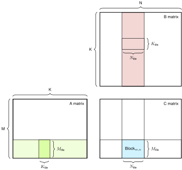
Tiling fundamentals
In listing 14, every iteration of the innermost loop fetches \(\GemmLeftOperandElement_{ik}\) and \(\GemmRightOperandElement_{kj}\), multiplies them, and updates \(\GemmOutputElement_{ij}\). When the matrices are large, the processor reloads values it used moments earlier, and each reload that misses on chip pays the DRAM penalty in latency and energy (Horowitz 2014; Sze et al. 2017).
Horowitz, Mark. 2014. “1.1 Computing’s Energy Problem (and What We Can Do about It).” 2014 IEEE International Solid-State Circuits Conference Digest of Technical Papers (ISSCC), 10–14. https://doi.org/10.1109/isscc.2014.6757323.
Performance benefits of tiling
Tiling processes one submatrix at a time, so that once a block is loaded it is reused many times before the loop moves on. Listing 16 demonstrates cache-friendly loop blocking: the loop bounds partition the matrices into tiles, and the hardware cache hierarchy keeps recently used tile data close to the compute units when access order has locality.
TILE_SIZE = 32  # Choose a tile size based on hardware constraints

# Cache blocking: partition data via loop bounds.
# Loads are implicit through the hardware cache hierarchy.
for i in range(0, N, TILE_SIZE):
    for j in range(0, N, TILE_SIZE):
        for k in range(0, N, TILE_SIZE):
            # Each tile computed independently
            for ii in range(i, min(i + TILE_SIZE, N)):
                for jj in range(j, min(j + TILE_SIZE, N)):
                    for kk in range(k, min(k + TILE_SIZE, N)):
                        C[ii, jj] += A[ii, kk] * B[kk, jj]
The restructuring produces a chain of effects. A small tile is revisited while it is still likely to be cached, so most operand references hit in L1/L2 or shared memory instead of DRAM. DRAM traffic falls as a result, and the processing units spend less time waiting for operands. When an untiled access pattern repeatedly fetches operands from lower memory tiers, that traffic can impose a bandwidth ceiling below the arithmetic ceiling.
Tiling methods
Tiling implementations differ along one axis, which is whether the hardware or the program decides what stays in fast memory. The two ends are implicit (cache) blocking and explicit (scratchpad) staging, and practical kernels often combine them.
Implicit (cache) blocking restructures only the loop bounds. The tiled matrix multiplication in listing 16 issues no explicit loads; its tile-shaped access pattern lets hardware caches reuse nearby values before they are evicted. It suits CPUs and GPUs with capable caches and large tensors that exceed fast-memory capacity.
Explicit (scratchpad) staging copies each tile into shared memory, a scratchpad, or registers and reorganizes the computation around the staged copy. It is the only option on accelerators whose fast memory is software managed, and it guarantees reuse that a cache might lose to eviction. Convolution is the classic case, because staging a filter once lets it serve many input regions without being refetched. Listing 17 loads blocks of \(\GemmLeftOperand\) and \(\GemmRightOperand\) into temporary fast storage and reuses them across the inner loops, including shortened boundary tiles when \(\SquareGemmDimension\) is not divisible by TILE_SIZE (the software counterpart of the fringe penalty that a fixed-size array pays in idle processing elements).
# Explicit tile staging: load data into fast
# temporary storage before the inner loops.
for i in range(0, N, TILE_SIZE):
    for j in range(0, N, TILE_SIZE):
        for k in range(0, N, TILE_SIZE):
            # Pseudocode: map these tile objects to fast memory
            A_tile = A[i : i + TILE_SIZE, k : k + TILE_SIZE]
            B_tile = B[k : k + TILE_SIZE, j : j + TILE_SIZE]

            # Reuse loaded tiles for all inner iterations
            for ii in range(A_tile.shape[0]):
                for jj in range(B_tile.shape[1]):
                    for kk in range(A_tile.shape[1]):
                        C[i + ii, j + jj] += (
                            A_tile[ii, kk] * B_tile[kk, jj]
                        )
Tiling challenges and trade-offs
Tiling improves performance only when the tile matches the locality budget of the hardware. If the tile is too small, memory fetches still dominate execution time because reuse is too limited. If the tile is too large, it exceeds fast memory and causes cache thrashing or scratchpad spills. Selecting the right tile size therefore directly determines computational efficiency and memory bandwidth usage.
The capacity test counts every buffer that is live at the same time. For the tile dimensions in algorithm 1, the operand blocks contain \(\GemmTileRowDimension \GemmTileInnerDimension\) and \(\GemmTileInnerDimension \GemmTileColumnDimension\) elements, while the output accumulator contains \(\GemmTileRowDimension \GemmTileColumnDimension\) elements. Suppose a hypothetical accelerator retains all three in one software-managed local store, uses FP16 operands and an FP32 accumulator, and loads only the current operand pair. Element storage size \(\ElementStorageSize\) is then 2 bytes for each operand and 4 bytes for each accumulator entry. After reserving space for other live state, the tile must satisfy \[ (2\text{ bytes})\GemmTileRowDimension \GemmTileInnerDimension+ (2\text{ bytes})\GemmTileInnerDimension \GemmTileColumnDimension+ (4\text{ bytes})\GemmTileRowDimension \GemmTileColumnDimension\le \text{available local bytes}. \tag{6}\] Keeping the output dimensions fixed while doubling the reduction tile doubles both operand buffers without changing the accumulator. Reject that larger candidate if the revised left-hand side of equation 6 exceeds the available capacity, even if its longer reduction amortizes accumulator handling over more products. Double buffering has the same operand-capacity effect at fixed tile dimensions: retaining the next \(\GemmLeftOperand\) and \(\GemmRightOperand\) tiles while computing the current pair requires a second copy of each operand buffer, while the running accumulator remains single buffered.
Actual storage tiers must be budgeted separately. A GPU kernel may stage operand tiles in shared memory while keeping output accumulators in thread registers; unused register capacity cannot make an oversized shared-memory allocation fit. Its shared-memory test counts the staged operand copies and any other shared state, while its register test counts accumulators, operand fragments, and temporary values across the participating threads. Passing both tests establishes capacity feasibility. It does not establish speed: alignment, bank conflicts, occupancy, synchronization, and measured traffic still determine whether the tile improves execution.
The tile choice also controls load balance. In architectures such as GPUs and TPUs, computations execute in parallel across thousands of processing units. If tiles are not evenly distributed, some units remain idle while others are overloaded, leading to suboptimal utilization of computational resources. Effective tile scheduling keeps parallel execution balanced and efficient.
Data movement remains a cost after tiling, even when another resource becomes the throughput limit. Although tiling reduces the number of slow memory accesses, transferring tiles between hierarchy levels still incurs latency and energy cost, especially when data falls from cache or scratchpad back to DRAM. Efficient memory prefetching and scheduling strategies minimize this residual movement and ensure that data is available when needed.
Hybrid tiling combines implicit blocking and explicit staging when neither alone captures the workload’s reuse, for example relying on caches for an outer tier while staging convolution weights explicitly in a scratchpad. Register blocking, double buffering, and hierarchical tiling extend the same locality principle at smaller and larger memory tiers. AI compilers and runtime systems such as TensorFlow XLA, TVM, and MLIR automatically select these tiling strategies based on hardware constraints, enabling fine-tuned performance optimization without manual intervention. Table 12 compares implicit, explicit, and hybrid tiling.
| Aspect | Implicit (Cache) Blocking | Explicit (Scratchpad) Staging | Hybrid tiling |
|---|---|---|---|
| Who Decides Residency | Hardware cache replacement policy | The program, through explicit copies into software-managed memory | Caches for some tiers, explicit copies for others |
| Optimization Focus | Loop bounds shaped so accesses stay within cache-sized blocks | Staging tiles and reordering computation around the staged copy | Matching each memory tier to the mechanism it supports |
| Memory usage | Improves cache locality and reduces DRAM access | Keeps frequently used data in fast memory for multiple iterations | Minimizes data movement while ensuring high reuse |
| Common use cases | Matrix multiplications, CNNs, self-attention in transformers | Convolutions, recurrent neural networks (RNNs), iterative computations | AI accelerators with hierarchical memory, mixed workloads |
| Performance gains | Reduced memory bandwidth requirements, better cache utilization | Lower memory fetch latency, improved data locality | Maximized efficiency across multiple hardware types |
| Challenges | Reuse is not guaranteed; eviction can discard a tile before it is reused | Can increase register pressure, requires loop restructuring | Complexity in tuning tile size and execution order dynamically |
| Best when | Hardware caches are capable and the working set exceeds fast memory | Fast memory is software managed or reuse must be guaranteed | Different memory tiers favor different mechanisms |
11.7.6 Memory-efficient tensor layouts
Stationary dataflows (section 11.7.4) and tiling determine which operands stay close to compute units and in what blocks; tensor layouts determine whether those operands can be accessed efficiently once they arrive. A well-chosen weight-stationary schedule still stalls if weights are laid out in a format that produces strided, non-coalesced memory fetches. Tensor layout is a kernel requirement. The physical ordering of multidimensional data in linear memory must match the memory access stride expected by the accelerator’s execution units, or the processor pays in memory stalls, cache underutilization, and redundant bus transactions.
Hardware accelerators fetch data from device memory in fixed-size transactions, typically 32 to 128 bytes per transaction. When compute units request non-contiguous addresses, each transaction delivers only a fraction of useful payload, degrading effective memory bandwidth. Aligning tensor layout with the execution model lets concurrent threads or SIMD lanes access nearby aligned locations in fewer transactions; the count depends on access width and device granularity (NVIDIA Corporation 2021).
Machine learning frameworks and compilers often manage this layout selection automatically. Optimization tools such as cuDNN for NVIDIA GPUs, XLA for TensorFlow and JAX, and MLIR-based compiler stacks transform tensor layouts as they lower operations to backend-specific kernels (NVIDIA Corporation 2021; Google 2025; Lattner et al. 2020). In high-level frameworks, layout transformations are typically applied transparently, but developers authoring custom kernels or targeting low-level APIs such as CUDA, Metal, or OpenCL must manage tensor formats directly.
In PyTorch, for example, view operations such as tensor.permute() adjust tensor strides without moving data in memory, requiring an explicit tensor.contiguous() call to materialize a packed buffer when a downstream kernel requires contiguous storage (PyTorch Contributors 2026). Conversely, TensorFlow defaults to channels-last (NHWC) for convolutional models on NVIDIA GPUs, warning that NCHW inputs introduce automatic transpose overhead when lowered to GPU kernels (TensorFlow Developers 2024). Hardware-optimized libraries such as cuDNN on GPUs and oneDNN on CPUs implement tailored memory formats to maximize cache line utilization and SIMD throughput. The governing principle is to treat memory layout as an intrinsic property of the backend execution path: the fastest tensor format is the one that minimizes layout conversion overhead and makes memory accesses contiguous across hardware execution units.
PyTorch Contributors. 2026. Tensor Views.
TensorFlow Developers. 2024. Optimize TensorFlow Performance Using the Profiler.
Channels-last layout
In an NHWC channels-last layout, the channel index varies fastest in a contiguous tensor, placing the channel values for each spatial coordinate adjacent in memory. The label names the order in which dimensions are laid out in memory, from slowest-varying to fastest-varying, so NCHW and NHWC hold the same values in different linear orders.
Consider an RGB image tensor of shape \((\text{Height}, \text{Width}, \text{Channels}) = (3, 3, 3)\). The elements \(\ImageTensorElement(\ImageRowIndex,\ImageColumnIndex,\ImageChannelIndex)\) are laid out in linear memory as follows: \[\begin{gather*} X(0,0,0), X(0,0,1), X(0,0,2), X(0,1,0), X(0,1,1), \\ X(0,1,2), X(0,2,0), X(0,2,1), X(0,2,2), \ldots \end{gather*}\]
All channel values for a given pixel are adjacent, and memory addresses advance across width before advancing down height. This layout supports vectorized execution when a compute kernel processes multiple channels simultaneously: CPU SIMD registers and GPU Tensor Cores can load contiguous channel vectors directly without intra-register shuffling.
The advantage of channels-last storage depends on the target operator and hardware unit. TensorFlow uses NHWC by default, whereas PyTorch provides a dedicated channels-last memory format that decouples logical dimension ordering from physical storage. Modern Tensor Core kernels in cuDNN favor NHWC because matrix-multiply units pack channel dimensions directly into accumulator tiles. When kernels require channel-contiguous inputs, passing an incompatible format forces the framework runtime to insert an explicit memory transpose, incurring a memory bandwidth penalty before computation begins.
Channels-first layout
In a contiguous NCHW channels-first layout, the spatial width index varies fastest, and all spatial values across an entire channel are stored contiguously before the next channel begins. Accelerators process data in parallel across thread warps or SIMD lanes; when consecutive threads in a warp access consecutive memory addresses, the memory controller coalesces those requests into fewer memory transactions (memory coalescing).23
23 Memory coalescing: The GPU hardware mechanism that combines memory requests from threads in a warp into transactions according to address locality, alignment, access width, and device granularity. Tensor layout therefore decides how many transactions a warp’s loads become, and whether a given layout helps depends on how the kernel assigns threads to tensor dimensions.
Consider the same RGB image tensor with dimensions reordered in channels-first order as \((\text{Channels}, \text{Height}, \text{Width}) = (3, 3, 3)\). Retaining \(\ImageTensorElement(\ImageRowIndex,\ImageColumnIndex,\ImageChannelIndex)\) as semantic coordinate notation, the data are stored in channels-first order as follows: \[\begin{gather*} X(0,0,0), X(0,1,0), X(0,2,0), X(1,0,0), X(1,1,0), X(1,2,0), \ldots, \\ X(0,0,1), X(0,1,1), X(0,2,1), \ldots, X(0,0,2), X(0,1,2), X(0,2,2), \ldots \end{gather*}\]
In this format, all red channel values for the entire image are stored first, followed by all green values, and then all blue values. This arrangement allows kernels that parallelize across spatial coordinates \((\ImageHeight, \ImageWidth)\) to issue coalesced reads along image rows, which suited earlier GPU convolution algorithms and SIMD execution pipelines (Chetlur et al. 2014).
Chetlur, Sharan, Cliff Woolley, Philippe Vandermersch, Jonathan Cohen, John Tran, Bryan Catanzaro, and Evan Shelhamer. 2014. “cuDNN: Efficient Primitives for Deep Learning.” arXiv Preprint arXiv:1410.0759.
24 NHWC vs. NCHW: NHWC lists dimensions as batch, height, width, channel; NCHW lists batch, channel, height, width. Physical memory format determines whether adjacent threads read adjacent addresses, so the performance effect is backend-specific. Layout-to-hardware mismatch is not a micro-optimization; it can create multi-fold performance gaps, especially when a conversion prevents Tensor Core convolution or fusion paths from being used.
The relative advantage of NCHW versus NHWC depends on how the underlying kernel maps computation to hardware threads. Convolutional layers evaluate filters across spatial and channel dimensions simultaneously. In classic direct or FFT-based convolutions, channels-first ordering enabled efficient spatial sliding without stride jumps. However, modern GEMM-lowered convolutions and Tensor Core pipelines map channel reduction directly to matrix multiply accumulators, favoring channels-last structures. When a model operates in NCHW but invokes a Tensor Core-optimized backend, the runtime must either run an unoptimized fallback kernel or dynamically transpose the tensor into NHWC, burning memory bandwidth in both cases.24
Comparing channels-last and channels-first layouts
Both channels-last (NHWC) and channels-first (NCHW) layouts address specific hardware access patterns, with their efficiency determined by whether a kernel parallelizes over spatial coordinates or vectorizes across channel dimensions. Layout choice directly governs cache line utilization, memory bus transaction count, and compute unit occupancy. Table 13 contrasts the performance trade-offs and hardware compatibility between these two approaches.
| Feature | Channels-Last (NHWC) | Channels-First (NCHW) |
|---|---|---|
| Memory storage order | Pixels are stored row-by-row, channel interleaved | All values for a given channel are stored together first |
| Best for | CPU loops, element-wise operations, many channels-last kernels | Many legacy GPU convolution paths and channel-first model code |
| Cache efficiency | High cache locality for sequential row/channel-last access | Can improve coalescing for channel-first kernels |
| Convolution performance | Often preferred by modern Tensor Core convolution/fusion paths | Efficient for older FP32 cuDNN paths and direct convolutions |
| Memory fetching | Good when kernels vectorize over adjacent channel data | Good when kernels process channel-major tiles |
| Default in frameworks | Common TensorFlow convention; PyTorch channels-last option | Common PyTorch tensor shape convention |
While compilers such as XLA, TensorRT, and PyTorch Inductor automate layout propagation and insert layout conversions when beneficial, format conversions are not free: transposing a tensor requires reading every element from memory and writing it back in a different order, consuming memory bandwidth without executing useful arithmetic. In production deployments, matching the model’s memory layout to the accelerator’s native kernel format eliminates these layout transformations entirely. Even when tensor layout is perfectly aligned with the hardware, however, executing operations as isolated kernels introduces a separate bottleneck: intermediate values must be exposed through global-memory buffers between operations, even when caches absorb some physical traffic. Resolving that bottleneck requires changing how operations are scheduled rather than how tensors are laid out.
11.7.7 Kernel fusion on the accelerator
Kernel fusion25 entered the book as a framework optimization that combines successive operations into a single kernel to avoid intermediate memory round trips. The LayerNorm analysis (notebook 11.8) shows why it matters on an accelerator. At 2.0 FLOP/byte, a standalone normalization kernel can reach at most 6.7 TFLOP/s, about 0.7 percent of the H100’s tensor peak, however its arithmetic is scheduled. The hardware questions are which intermediates fusion removes from the memory bus and what the fused kernel costs in registers and occupancy.
25 Kernel fusion: Separate GPU kernels expose intermediate results through device memory, although caches can absorb some traffic. A fused kernel can keep intermediates in registers or local storage and avoid corresponding external write/read cycles. The resulting speedup depends on cache behavior, occupancy, launch overhead, and whether memory traffic was the bottleneck; it is not necessarily proportional to the byte reduction.
↩︎ Kernel fusion (also called operator fusion), with its LayerNorm, dropout, and ReLU example and the traffic count for unfused versus fused chains, is established in The memory wall and kernel fusion.
The case for fusion rests on a traffic count. Run as separate kernels, a chain of three elementwise operations writes each intermediate result to device memory and reads it back for the next operation, whereas a fused kernel reads the input once, keeps the intermediates in registers or on-chip SRAM, and writes only the final output, which cuts idealized external traffic by roughly 3\(\times\). On an accelerator the saving matters most for elementwise operators, whose arithmetic intensity sits far below one FLOP per byte, so moving each intermediate across the memory bus takes longer than computing it (Jia et al. 2019). Fused execution also shortens the lifetime of intermediate buffers, although an optimizing runtime can often reuse those buffers anyway; what fusion guarantees is the removed write and read for each eliminated intermediate, and how much of that removed traffic would have reached DRAM depends on cache behavior.
Performance benefits and constraints
Because high-bandwidth memory is the scarce resource on GPUs and TPUs, eliminating redundant memory transactions translates directly into higher compute utilization (NVIDIA Corporation 2020a). Not all operations can be fused arbitrarily, however. Element-wise operations and frozen inference normalization are strong candidates because their computations do not require batch-wide reductions, whereas training-mode batch normalization computes batch statistics and is not purely element-wise. Matrix multiplications and convolutions constrain fusion further because they involve reductions and large data movement; compilers routinely fuse them with element-wise epilogues such as bias or activation, yet cannot freely merge them with unrelated global operations.
Even when two operators are algebraically compatible, register pressure bounds how aggressively they should be fused. Keeping intermediate values in registers eliminates redundant memory writes, but if a fused kernel exceeds the available registers per thread, the compiler spills excess values to per-thread local memory backed by device DRAM, adding latency that can negate the benefits of fusion. On GPUs, where thread occupancy (the number of threads active in parallel) is bounded by the register file, excessive fusion can also starve parallelism. Different accelerators and compilers therefore strike different balances: NVIDIA GPUs favor warp-level parallelism where element-wise epilogue fusion is straightforward (NVIDIA Corporation 2020a), while TPUs prioritize systolic-array execution coupled to vector post-processing (Jouppi et al. 2017), and compiler stacks such as TVM, XLA, TensorRT, and MLIR use graph rewrites and engine-building heuristics to weigh memory savings against register and occupancy limits (Chen et al. 2018; Google 2025; NVIDIA 2024b; Lattner et al. 2020). When debugging performance regressions or modifying models frequently, frameworks also allow developers to disable fusion selectively so that memory savings, register usage, and hardware execution constraints can be evaluated independently.
Checkpoint 11.4: Data movement and kernel fusion
The dataflow building blocks are now in place: data locality, tensor layout, and kernel fusion. These fusion decisions are ultimately about data locality, which ties together the chapter’s core data movement strategies:
11.7.8 Applying mapping strategies to neural networks
While section 11.5.5 diagnosed how convolutional networks, transformers, and multilayer perceptrons stress memory subsystems, the mapping strategies above provide the systems remedies. Mapping is a systematic search over loop permutations, tiling factors, and stationarity policies that maximizes data reuse under hard SRAM and register constraints. Because each model family presents a distinct ratio of weights to activations and differing opportunities for temporal locality, optimal mapping policies diverge across workloads. Convolutional networks exploit 2D spatial weight reuse across receptive fields; transformers split between compute-bound matrix multiplications during prefill and bandwidth-bound KV-cache streaming during autoregressive decoding; and dense MLPs demand blocked GEMM execution across batch dimensions. Table 14 consolidates how dataflow, memory layout, kernel fusion, and tiling align with these three architectural archetypes.
Convolutional neural networks (ResNet-50)
For ResNet-50 and similar CNNs, a key mapping opportunity is spatial weight reuse. A small filter is applied across many spatial locations, so its weights participate in many multiply-accumulate operations. Weight-stationary mappings can capture that reuse by retaining filter tiles locally, while row-stationary or output-stationary mappings may better balance activation and partial-sum traffic on other architectures. Favorable convolution shapes can achieve high arithmetic intensity, which makes them well suited to matrix and systolic execution paths. The model family does not determine one universal dataflow: layer shape, batch size, local-storage capacity, and the target’s supported kernels decide which reuse pattern is worth retaining.
| Property or technique | CNNs | Transformers | MLPs | Rationale |
|---|---|---|---|---|
| Weight size | Small, reused | Large, usually dense; sparse in MoE or pruned variants | Large, dense | Sets whether weights can stay on chip or must stream from HBM on every use. |
| Activation reuse | High | Low to medium | Low | Sets how much each loaded activation is worth keeping in local storage. |
| Memory access pattern | Spatial locality | Mostly regular GEMM plus KV-cache and attention traffic | Regular, sequential (streamed) | Regular patterns tile and prefetch well; KV-cache reads grow with context length. |
| Potential memory pressure | Feature-map movement | Memory capacity and bandwidth | Bandwidth at low batch | Starting hypotheses that execution phase, batch size, and data movement can change, not fixed bottleneck classifications. |
| Dataflow strategy | Weight, row, or output stationary | Phase- and kernel-dependent | Weight or output stationary | CNNs expose filter and spatial reuse; transformer attention and MLP blocks impose different traffic; dense MLPs reuse weights across a batch and accumulate outputs. |
| Memory-aware tensor layouts | Backend-dependent (channels-last on Tensor Core paths, NCHW on older FP32 paths) | Backend-dependent (row-major activations typical) | Row-major typical | Layout choice depends on backend kernel path and precision mode (section 11.7.6 compares the layouts); the entries name common defaults, not universal prescriptions. |
| Kernel Fusion | Convolution + Activation | Fused Attention | GEMM Fusion | CNNs optimize convolution+activation fusion; Transformers fuse attention mechanisms; MLPs benefit from fused matrix multiplications. |
| Tiling for Memory Efficiency | Explicit staging of feature-map tiles | Explicit staging of attention blocks | Blocked GEMM | CNNs stage feature-map subregions in on-chip SRAM; transformers stage query and key/value blocks in fused attention; MLPs block large matrix multiplications, implicitly or explicitly. |
This spatial regularity also enables aggressive fusion and tiling. For inference with frozen BatchNorm statistics, compilers can fold or fuse convolution, normalization, and activation to avoid unnecessary intermediate writes. Training-mode BatchNorm requires reductions over batch statistics and does not have the same element-wise structure that permits fusion. Spatial tiling partitions the feature map into subregions sized to fit within on-chip SRAM, so the fused kernel processes each tile from fast memory before moving to the next.
Transformer architectures (GPT-2/Llama)
Transformer mapping depends on execution phase. During training and prefill, attention creates large intermediate matrices unless a tiled implementation avoids materializing them; during autoregressive decoding, attention reads the growing key-value (KV) cache. Each new query vector must access the stored key and value pairs across the preceding sequence. As sequences grow, the full KV cache usually lives in HBM or device DRAM, while attention kernels tile active blocks through SRAM, registers, or shared memory. This access pattern motivates staging active K/V tiles in SRAM so attention consumes them from fast local storage. During training and prefill, the memory traffic created by standard attention implementations similarly explains why fused attention kernels, such as FlashAttention (Dao et al. 2022), can deliver large performance gains: they tile the query-key product, softmax, and value summation through on-chip SRAM so the full attention matrix never reaches HBM, while the \(\mathcal{O}(\SequenceLength^2)\) computation is preserved (FlashAttention: IO-aware attention optimization develops the algorithm).
Multilayer perceptrons and DLRM
MLPs present the most straightforward mapping problem because their computation reduces largely to dense GEMM.26 Each fully connected layer multiplies an activation matrix by a weight matrix. The weight matrix is fixed across samples, so batching reuses each loaded weight across more activations and raises arithmetic intensity. A batch size of one provides little cross-sample weight reuse and often leaves wide matrix engines underused, while larger batches can move execution toward the compute-bound regime.
26 GEMM: The operation \(\GemmOutputMatrix= \GemmProductScale\GemmLeftOperand\GemmRightOperand+ \GemmAccumulatorScale\GemmOutputMatrix\), with scalars \(\GemmProductScale\) and \(\GemmAccumulatorScale\), is the dense linear-algebra primitive that many deep-learning layers lower to. Optimized GEMM libraries such as cuBLAS and oneDNN use register blocking, vectorization, and hierarchical tiling to approach hardware limits on favorable shapes (NVIDIA 2024a; Intel Corporation 2021b). Modern AI accelerators are heavily specialized for GEMM-like tiles: Tensor Cores, systolic arrays, and matrix extensions all exist to accelerate this primitive, which is why GEMM performance is an important predictor of end-to-end throughput across architectures.
NVIDIA. 2024a. cuBLAS: CUDA Basic Linear Algebra Subprograms.
Intel Corporation. 2021b. oneDNN: Intel’s Deep Learning Neural Network Library.
↪ How GEMM arithmetic intensity scales with matrix dimension is collected for reference in General matrix multiply (GEMM).
Naumov, Maxim, Dheevatsa Mudigere, Hao-Jun Michael Shi, Jianyu Huang, Narayanan Sundaraman, Jongsoo Park, Xiaodong Wang, et al. 2019. “Deep Learning Recommendation Model for Personalization and Recommendation Systems.” arXiv Preprint arXiv:1906.00091.
Because MLP layers are typically followed by activation functions and bias additions, GEMM fusion combines these steps into a single kernel, avoiding intermediate memory writes. Blocked tiling partitions the large matrix multiplications into sub-blocks sized for the accelerator’s shared memory, ensuring high cache utilization throughout computation. The simplicity of the MLP mapping, dominated by a single primitive with predictable access patterns, is precisely why hardware vendors optimize GEMM libraries so aggressively: gains in GEMM performance translate directly to MLP throughput. DLRM is not purely an MLP workload, however. Its large sparse embedding tables and feature-interaction stage can dominate capacity and memory traffic, so the dense mapping described here applies to its bottom and top MLP towers rather than to the entire model (Naumov et al. 2019).
11.7.9 Hybrid mapping strategies
The preceding architectural subsections treat each architecture in isolation, but real models rarely consist of a single layer type. A vision transformer, for example, combines a patch embedding stage, self-attention layers, and MLP blocks (Dosovitskiy et al. 2021). Those layers create different reuse patterns: the embedding stage can benefit from weight-stationary mapping, attention emphasizes activation movement and tiling, and MLP blocks demand blocked GEMM tiling and fusion. No single dataflow strategy is optimal across all these layers, so hardware mapping becomes hybrid and layer-specific.
Dosovitskiy, Alexey, Lucas Beyer, Alexander Kolesnikov, Dirk Weissenborn, Xiaohua Zhai, Thomas Unterthiner, Mostafa Dehghani, et al. 2021. “An Image Is Worth 16x16 Words: Transformers for Image Recognition at Scale.” International Conference on Learning Representations (ICLR).
Hybrid mapping addresses this heterogeneity by allowing the accelerator to switch strategies at layer boundaries. Each layer presents a different balance of compute intensity, data reuse, and memory access pattern, and the optimal mapping must shift accordingly (Sze et al. 2017). Rather than committing to one dataflow for the entire model, hybrid approaches consider weight stationary execution when weights can be reused locally, input-stationary execution when activation reuse justifies its storage, and output stationary execution when partial-sum traffic is costly. Layer dimensions and available local memory determine which candidate pays off.
TPU-style systolic arrays, NVIDIA GPUs, and tile-based accelerator designs expose different combinations of local memory, tensor layouts, fusion, and scheduling controls, allowing compilers and runtimes to choose layer-specific strategies rather than one global dataflow for the whole model (Jouppi et al. 2023; NVIDIA Corporation 2020a; Chen et al. 2018). These implementations depend on programmable memory hierarchies, efficient interconnects, and specialized execution pipelines. However, hybrid mapping remains a design-time optimization: in production workloads, execution conditions change dynamically due to varying input sizes, memory contention, and hardware resource availability. Machine learning compilers and runtime systems extend these static mapping choices by introducing dynamic scheduling, memory optimizations, and automatic tuning, ensuring that deep learning workloads operate efficiently across diverse accelerators and deployment environments.
Self-Check: Question
In neural network hardware mapping, what distinguishes a spatial mapping decision from a temporal mapping decision?
- Spatial mapping refers to compiling graph IR, whereas temporal mapping refers to runtime CUDA kernel launches
- Spatial mapping determines precision formats (FP16 vs INT8), whereas temporal mapping determines memory allocation sizes
- Spatial mapping assigns computational tasks to specific physical execution units (e.g., PEs or SMs) simultaneously in parallel, whereas temporal mapping determines the execution ordering and loop scheduling over time on those units
- Spatial mapping operates only on convolutional layers, whereas temporal mapping operates only on transformer attention layers
Contrast the data movement mechanics and primary use cases of Weight-Stationary (WS) and Output-Stationary (OS) systolic array dataflows.
When mapping a tensor computation to a multi-level memory hierarchy, what is the primary objective optimized by tiling, whether through implicit cache blocking or explicit scratchpad staging?
- Maximizing the total number of intermediate tensors written to host DDR memory
- Maximizing data reuse in the fastest, closest memory tiers (registers and SRAM) to minimize traffic to slower, energy-expensive DRAM
- Ensuring every warp thread executes different instruction streams simultaneously
- Converting all 2D matrix multiplications into 1D scalar operations
Why do modern deep learning libraries (e.g., cuDNN, TensorRT) strongly prefer the Channels-Last (NHWC) tensor layout over Channels-First (NCHW) when executing convolutions on NVIDIA Tensor Cores?
- NHWC eliminates the need for spatial convolutions by flattening images into 1D vectors
- NCHW requires floating-point numbers to be stored in big-endian byte order
- NHWC reduces model parameter count by sharing channel weights across batches
- NHWC places channel values for a given spatial location in contiguous memory, aligning with the packed vector/matrix multiply requirements of Tensor Cores
Explain the mechanism of vertical kernel fusion (e.g., fusing
Conv2D\(\to\)BatchNorm\(\to\)ReLU), and identify both its performance benefit and its primary architectural constraint.True or False: Row-Stationary (RS) dataflow, as implemented in architectures like Eyeriss, keeps only the final output activation stationary in registers while streaming 2D convolutional filter rows and input rows from DRAM on every clock cycle.
11.8 Compilers and Runtimes
The roofline gives each ResNet-50 layer a ceiling, and hardware mapping showed which schedules can approach it, but neither reaches the silicon by itself. Every layer needs a tiling, a stationary operand, a tensor layout, a precision for the activations it reads and writes, and a fusion boundary, and the resulting plan must then run on a device whose input shapes, free memory, and clock rate change while it serves. Across a whole model these choices number in the thousands, which is why compilers and runtimes, not engineers, make them. Graph capture and dispatch overhead, which decide how a model reaches a compiler, belong to ML Frameworks, and the choice of a deployment runtime for a service belongs to Inference Runtime Selection. What remains here is lowering, the path from a captured graph to the accelerator’s units, and the runtime that executes the result. The decode floors this chapter quotes for GPT-2 XL assume that the step is launched as a captured graph (Graph capture and JIT compilation); executed one eager kernel at a time, launch overhead rather than memory bandwidth would set the floor.
A single convolution can be implemented with dozens of valid tiling strategies, kernel variants, and memory layouts, most of which perform poorly on a given target. Machine learning compilers navigate this space by translating high-level dataflow representations into target-specific executable code, making the mapping and dataflow decisions of the preceding sections automatically. Compiling ResNet-50 for GPU inference illustrates the core compiler stages:
- Graph optimization fuses repeated Conv2D-BatchNorm-ReLU patterns into single compound kernels, eliminating intermediate round-trips to HBM.
- Kernel selection chooses specialized Tensor Core implementations for compatible matrix multiplications, exploiting the high arithmetic intensity of dense convolutions.
- Memory planning determines activation lifetimes to safely overlap and reuse intermediate buffer allocations.
- Computation scheduling pipelines memory copies with execution across independent hardware queues to hide data transfer latencies.
↩︎ Graph compilation, kernel fusion, and framework dispatch overhead are established in Execution: From Graphs to Kernels.
On the reference H100, the modeled batch-one forward pass falls from 3.53 ms in an eager framework to 0.33 ms as a compiled FP16 engine, a 10.6× improvement without altering the model’s mathematical output. The arithmetic per image is unchanged. The gain comes from fusing the network’s 174 framework kernels into 56 and launching them as one graph instead of one Python dispatch at a time, which removes the fixed cost that dominates a single image. That answers the question the chapter opened with. The INT8 arithmetic for one image takes about 4 μs on the H100 (8 μs at FP16), so even the compiled pass spends almost all of its time on launch and overhead; batch-one latency sits on the overhead floor rather than on either roofline ceiling, which is why halving the arithmetic barely moves it. The latencies are modeled rather than measured, and Inference Runtime Selection separates the same gap into the contribution of each runtime, but the mechanism is general. Graph rewrites, kernel selection, memory planning, and scheduling systematically apply kernel fusion (section 11.7.7) and memory-efficient tiling (section 11.7.5.1) to convert theoretical hardware FLOP/s into delivered throughput (Chen et al. 2018; NVIDIA 2024b).
11.8.1 ML compiler design
Machine learning compilers specialize conventional compilation techniques for programs expressed as tensor graphs and operator libraries. General-purpose compilers optimize scalar control flow, vector instructions, register allocation, and cache locality; ML compiler stacks operate at a higher semantic level, optimizing graph topology, tensor memory layouts, shape specialization, accelerator kernel dispatch, and inter-device execution planning (Li et al. 2021). Table 15 contrasts the emphasis of these two compiler layers. The boundary is complementary rather than disjoint: an ML compiler stack lowers high-level tensor operations into intermediate representations that feed into an LLVM, GPU, or vendor-specific backend.
Li, Mingzhen, Yi Liu, Xiaoyan Liu, Qingxiao Sun, Xin You, Hailong Yang, Zhongzhi Luan, Lin Gan, Guangwen Yang, and Depei Qian. 2021. “The Deep Learning Compiler: A Comprehensive Survey.” IEEE Transactions on Parallel and Distributed Systems 32 (3): 708–27. https://doi.org/10.1109/tpds.2020.3030548.
| Aspect | Traditional compiler | Machine learning compiler |
|---|---|---|
| Input representation | Source or intermediate-representation program | Tensor graph or tensor-level intermediate representation |
| Execution Model | Control flow, loops, threads, vectors, and tasks | Tensor operators, kernels, graphs, and accelerator streams |
| Optimization priorities | Instruction selection, loop transforms, vectorization, registers | Graph rewrites, fusion, layouts, shapes, and kernel selection |
| Memory management | Objects, stack/heap, caches, locality, and prefetching | Tensor lifetimes, buffer reuse, layouts, tiling, and device transfers |
| Target Hardware | CPUs, GPUs, and other programmable targets | CPUs, GPUs, TPUs, and custom accelerators |
| Compilation output | Machine code or lower-level intermediate representation | Kernels plus a hardware-specific graph or execution plan |
The distinction in table 15 explains why compiler configuration dictates delivered performance even when the underlying neural network code remains unmodified. ML compilers manage the translation layer between high-level tensor operations and hardware execution units; when this mapping fails to expose reuse or efficient access, execution can be limited by memory traffic, latency, or insufficient parallel work.
11.8.2 ML compilation pipeline
Machine learning models defined in modern frameworks are represented as high-level dataflow graphs describing operations on multidimensional tensors. Lowering these representations into executable code for CPUs, GPUs, TPUs, or custom ASICs requires an ML compilation pipeline (Chen et al. 2018; Google 2025; Lattner et al. 2020). A standard compilation pipeline adds a fifth stage, code generation, to the four that the ResNet-50 example illustrated, emitting target-specific machine instructions, assembly, or interpreted bytecode. Across these stages, the compiler applies the dataflow strategies developed in section 11.7.3: kernel fusion, memory tiling, and compute placement. Hardware acceleration delivers its theoretical throughput only when these compiler-driven transformations expose sufficient arithmetic intensity and align memory access with the hardware hierarchy.
Graph optimization
Machine learning frameworks represent models as high-level computation graphs, where nodes represent mathematical operators (such as convolutions, matrix multiplications, and activations) and directed edges represent tensor data dependencies. Executing each operator as a separate kernel can incur intermediate-buffer traffic and repeated launches. An edge denotes a dependency, not necessarily a new allocation or an off-chip transfer, and asynchronous dependencies need not synchronize the host. When intermediate materialization and dispatch dominate execution, graph transformations can remove substantial overhead.
Graph optimization transforms this computation graph into an efficient execution plan before hardware code generation (Chen et al. 2018; Jia et al. 2019). Working primarily at a target-independent intermediate representation (IR) level before lowering (section 11.8.2.5), graph passes apply four core transformations. Kernel fusion merges adjacent operations into a single compound kernel to eliminate off-chip memory round-trips and launch overheads: in convolutional networks, fusing Conv2D, batch normalization with frozen inference statistics, and ReLU keeps activations in local registers or shared SRAM throughout the sequence (section 11.7.7), while in transformers, pattern matchers replace multi-operator self-attention subgraphs (score matrix multiplication, scaling, masking, softmax, and multiplication by the value matrix) with IO-aware attention kernels that keep active tiles and running reduction statistics in fast on-chip memory (Dao et al. 2022). Redundant computation elimination and constant folding remove work that need not happen at runtime at all, folding frozen normalization parameters into the weights and biases of the preceding linear or convolutional layer (Compression-specific fusion) while pruning dead subgraphs and merging identical parallel paths through common subexpression elimination.
Jia, Zhihao, James Thomas, Todd Warszawski, Mingyu Gao, Matei Zaharia, and Alex Aiken. 2019. “Optimizing DNN Computation with Relaxed Graph Substitutions.” Proceedings of Machine Learning and Systems (MLSys).
Dao, T., D. Y. Fu, S. Ermon, A. Rudra, and C. Ré. 2022. “FlashAttention: Fast and Memory-Efficient Exact Attention with IO-Awareness.” Advances in Neural Information Processing Systems (NeurIPS) 35: 16344–59. https://doi.org/10.52202/068431-1189.
The remaining two passes reduce data movement and live memory footprint without changing the operator set. Algebraic simplification and layout adjustments reorder mathematically equivalent operations—pushing transpositions through elementwise ops or canceling them against inverse permutations—to avoid runtime reshape traffic, while memory-aware node reordering evaluates topological sorts of the dependency graph and schedules independent operations so intermediate activations are consumed and deallocated promptly before memory pressure forces spills to host DRAM. Production compilers execute these rewrites through pattern-matching rules, producing a coarse-grained execution graph aligned with the accelerator’s bandwidth constraints before binding each node to a concrete hardware routine.
Kernel selection
Kernel selection binds each node in the optimized graph to a concrete hardware implementation. Accelerators provide dozens of valid kernel implementations for a single tensor operation, each parameterized by tile dimensions, thread block configurations, memory staging patterns, and target precision. Choosing the optimal kernel determines whether the execution engine achieves high compute utilization or stalls on uncoalesced memory accesses and pipeline bubbles (Chen et al. 2018; Zheng et al. 2020).
In most production pipelines, compilers draw from vendor-optimized kernel libraries (NVIDIA’s cuDNN and cuBLAS for GPUs, Intel’s oneDNN for x86) rather than synthesizing kernels from scratch. These libraries encode microarchitectural details such as register file capacity, cache latency, and vector lane width, so the compiler can invoke pre-tuned implementations.
AI compilers trade compilation time against execution speed across three strategies when choosing among candidate kernels, with numerical precision constraining all three. Rule-based selection is the fastest at compile time, relying on static heuristics over tensor shapes, alignment, data types, and target support to pick implementations such as a Tensor Core GEMM without benchmarking a large candidate set, at the risk of missing faster configurations on irregular shapes. Cost-model selection refines that choice without running hardware benchmarks by estimating kernel latency, register pressure, cache hit rates, and arithmetic intensity with analytical models that prune unpromising candidates (Lattner et al. 2020). When compilation budgets allow hardware measurement, profile-guided selection benchmarks candidates directly on the target device: autotuners such as TVM’s AutoTVM and Ansor search over tile sizes, unrolling factors, and thread configurations to converge on the fastest implementation (Chen et al. 2018; Zheng et al. 2020), and TensorRT similarly times candidate tactics against the target batch sizes. Across all three strategies, precision-aware constraints govern which candidates are legal: inference can use lower-precision paths after quality validation, but selecting INT8 without appropriate range handling degrades accuracy, whereas selecting a wider path unnecessarily forgoes available throughput.
Lattner, Chris, Mehdi Amini, Uday Bondhugula, Albert Cohen, Andy Davis, Jacques Pienaar, River Riddle, Tatiana Shpeisman, Nicolas Vasilache, and Oleksandr Zinenko. 2020. “MLIR: Scaling Compiler Infrastructure for Domain Specific Computation.” 2021 IEEE/ACM International Symposium on Code Generation and Optimization (CGO), 2–14. https://doi.org/10.1109/cgo51591.2021.9370308.
Memory planning
Memory planning assigns physical storage locations, buffer offsets, and tensor lifetimes across the accelerator’s memory hierarchy (Roesch et al. 2018; Chen et al. 2018). High-performance execution plans fail if memory management introduces uncoalesced memory transactions, bank conflicts, or unnecessary memory allocations that exhaust accelerator memory, so the compiler coordinates three core memory management mechanisms.
Google. 2025. XLA: Optimizing Compiler for Machine Learning.
Tensor layout optimization chooses the physical arrangement of tensor dimensions that each kernel needs for coalesced access and vectorization, such as channels-last NHWC for Tensor Core convolutions (section 11.7.6) (NVIDIA Corporation 2021; Google 2025). Compilers perform layout assignment globally across the graph to prevent back-to-back layout transformation kernels that consume memory bandwidth.
Liveness analysis and buffer reuse prevent out-of-memory errors by sharing physical memory across non-overlapping tensors. Deep neural networks generate dozens of intermediate activation tensors during forward propagation. Allocating a unique memory buffer for every tensor would quickly exceed the capacity of device memory (such as 16 to 80 GB on typical accelerator GPUs). The compiler analyzes the graph to compute the liveness interval of each tensor, from its generation to the completion of its last consumer. By modeling memory allocation as an interval graph coloring or 2D bin-packing problem, the compiler assigns multiple non-overlapping intermediate tensors to the same physical memory offsets (Roesch et al. 2018). This static reuse reduces peak device memory requirements to the working set size of concurrently active tensors, avoiding runtime allocation overhead and fragmentation.
Roesch, Jared, Steven Lyubomirsky, Logan Weber, Josh Pollock, Marisa Kirisame, Tianqi Chen, and Zachary Tatlock. 2018. “Relay: A New IR for Machine Learning Frameworks.” Proceedings of the 2nd ACM SIGPLAN International Workshop on Machine Learning and Programming Languages, 58–68. https://doi.org/10.1145/3211346.3211348.
Memory hierarchy placement optimizes the staging of data between external memory (HBM or GDDR) and on-chip scratchpad memories (SRAM or shared memory). External memory bandwidth is a scarce resource; moving intermediate tiles back and forth across the memory bus creates memory-bound stalls. Compilers synthesize tiling parameters that guarantee intermediate blocks remain resident in on-chip SRAM until all local compute operations complete, minimizing round-trip traffic across the memory bus. With memory layouts fixed and buffer addresses assigned, the compiler schedules operation execution across hardware compute resources.
Computation scheduling
Computation scheduling determines the execution timeline and hardware resource binding for operations in the compiled graph (Zheng et al. 2020). Modern accelerators feature deep hardware pipelines, multiple independent compute engines, and dedicated DMA copy engines. Effective scheduling coordinates these resources across three distinct architectural dimensions to maximize hardware occupancy, preserve data dependencies, and prevent pipeline stalls (Chen et al. 2018).
Norrie, Thomas, Nishant Patil, Doe Hyun Yoon, George Kurian, Sheng Li, James Laudon, Cliff Young, Norman Jouppi, and David Patterson. 2021. “The Design Process for Google’s Training Chips: TPUv2 and TPUv3.” IEEE Micro 41 (2): 56–63. https://doi.org/10.1109/mm.2021.3058217.
Task partitioning maps computational subgraphs onto the target’s physical execution units. On GPUs, computations are partitioned into grids of thread blocks dispatched across Streaming Multiprocessors (SMs). On TPUs, matrix multiplications are partitioned into tile sequences matched to the physical dimensions of systolic arrays (e.g., \(128 \times 128\) or \(256 \times 256\) processing elements) (Norrie et al. 2021). On CPUs, tasks are split into thread pools matching physical cores and vectorized to fill SIMD registers.
Execution ordering resolves dependencies while minimizing live memory pressure. Operations that depend on prior results must wait for producer kernels to complete, but independent branches (such as multi-head attention projections or parallel residual paths) can execute concurrently or interleave to maintain uniform compute utilization. Compilers analyze the dependency graph to schedule operations in an order that keeps compute pipelines full while keeping activation lifetimes short, preventing buffer bloat.
Asynchronous overlap hides memory latency by executing data transfers concurrently with compute kernels. Accelerators feature dedicated DMA engines that operate independently of arithmetic pipelines. Compilers exploit this architectural separation by scheduling memory transfers (such as host-to-device weights or inter-accelerator halo exchanges) in separate hardware queues or CUDA streams, overlapping transfer latency behind long-running compute operations (Chen et al. 2018; NVIDIA 2024b). When compute and transfer overlap completely, data movement costs are hidden behind arithmetic execution. Poor scheduling instead introduces execution bubbles where arithmetic units sit idle waiting for kernel dispatches or serialized data copies, so synchronizing kernels via explicit compiler-generated events and stream schedules ensures the hardware sustains continuous execution without CPU driver intervention (NVIDIA 2024b; Zheng et al. 2020).
Chen, Tianqi, Thierry Moreau, Ziheng Jiang, Lianmin Zheng, Eddie Q. Yan, Haichen Shen, Meghan Cowan, et al. 2018. “TVM: An Automated End-to-End Optimizing Compiler for Deep Learning.” Proceedings of the 13th USENIX Symposium on Operating Systems Design and Implementation (OSDI ’18), 578–94.
NVIDIA. 2024b. NVIDIA TensorRT: Programmable Inference Accelerator.
Zheng, Lianmin, Chengfan Jia, Minmin Sun, Zhao Wu, Cody Hao Yu, Ameer Haj-Ali, Yida Wang, et al. 2020. “Ansor: Generating High-Performance Tensor Programs for Deep Learning.” Proceedings of the 14th USENIX Symposium on Operating Systems Design and Implementation (OSDI), 863–79.
Code generation
With scheduling complete, the final compilation stage translates the scheduled execution plan into target-specific machine instructions. Code generation applies traditional backend compiler passes (instruction selection, register allocation, instruction scheduling, and peephole optimization) tailored to accelerator architectures.
Instruction selection for ML targets must emit instructions that directly engage specialized matrix ISA extensions. On NVIDIA GPUs, code generators emit PTX instructions such as mma.sync.aligned to invoke Tensor Cores directly, as shown in listing 13. On Intel CPUs with Advanced Matrix Extensions (AMX), the backend targets tile-multiply instructions operating on 2D register tiles. On Arm architectures with the Scalable Matrix Extension (SME), the target is outer-product accumulation across scalable vector tiles. A backend that emits generic floating-point vector instructions instead of these matrix extensions leaves the primary compute engines idle, reducing effective throughput by an order of magnitude. For CPUs and GPUs, compilers emit machine code or optimized assembly; for TPUs, field-programmable gate arrays (FPGAs),27 and proprietary NPUs, the output is often an optimized bytecode or binary execution package executed by a specialized hardware runtime.
27 Field-programmable gate array: “Field-programmable” means the logic fabric is configurable after manufacturing, contrasting with fixed-function ASICs. FPGAs can improve performance for latency-sensitive data center services by implementing custom pipelines matched to a particular workload (Putnam et al. 2014). This reconfigurability makes FPGAs attractive for rapidly evolving ML architectures where committing to an ASIC risks obsolescence, but the requirement for hardware description languages (Verilog/VHDL) and compilation times measured in hours creates a productivity barrier that limits adoption to deployments where the efficiency benefit justifies the engineering cost.
Putnam, Andrew, Adrian M. Caulfield, Eric S. Chung, Derek Chiou, Kypros Constantinides, John Demme, Hadi Esmaeilzadeh, et al. 2014. “A Reconfigurable Fabric for Accelerating Large-Scale Datacenter Services.” ACM SIGARCH Computer Architecture News 42 (3): 13–24. https://doi.org/10.1145/2678373.2665678.
11.8.3 Runtime support
A compiler transforms a high-level model into an execution plan tailored to target hardware, but that plan embeds static assumptions about runtime conditions: tensor shapes, workspace allocation limits, device capabilities, and execution concurrency. Ahead-of-time (AOT) compilation optimizes graph structures, fusion boundaries, and memory layouts for fixed shapes and known hardware configurations. While just-in-time (JIT) compilation can compile specialized variants dynamically as new shapes arrive, each compiled kernel still executes a fixed execution plan. Production serving breaks those assumptions: request arrival rates fluctuate, batch sizes vary, several inference workloads compete for shared accelerator memory, and thermal throttling can pull clock frequencies below their rated values. Request batching and admission control belong to the serving layer (Model Serving); the concern here is how the accelerator runtime dispatches compiled execution plans once a batch reaches the hardware.
An AI runtime bridges static graph compilation and the dynamic realities of accelerator execution. Compilers optimize and lower computational graphs under fixed structural assumptions, but production systems encounter variable batch sizes, fluctuating sequence lengths, and constrained memory budgets. The runtime executes compiled engines while managing input-dependent tensor shapes, device-memory buffers and workspace, asynchronous hardware streams, and precompiled execution profiles. In production inference stacks such as NVIDIA TensorRT, the offline builder optimizes the network and benchmarks candidate tactics to construct an execution engine, while the runtime engine binds input buffers, selects valid optimization profiles, and dispatches kernels to the accelerator (NVIDIA Corporation 2026a, 2026b).
NVIDIA Corporation. 2026a. How TensorRT Works.
NVIDIA Corporation. 2026b. Working with Dynamic Shapes.
Huang, Y., Y. Cheng, A. Bapna, O. Firat, D. Chen, M. X. Chen, H. Lee, et al. 2019. “GPipe: Efficient Training of Giant Neural Networks Using Pipeline Parallelism.” Advances in Neural Information Processing Systems (NeurIPS) 32: 103–12.
Mirhoseini, Azalia, Hieu Pham, Quoc V. Le, Benoit Steiner, Rasmus Larsen, Yuefeng Zhou, Naveen Kumar, Mohammad Norouzi, Samy Bengio, and Jeff Dean. 2017. “Device Placement Optimization with Reinforcement Learning.” International Conference on Machine Learning (ICML) 70: 2430–39.
This execution lifecycle spans three core responsibilities. First, the runtime selects and dispatches precompiled kernel variants matched to runtime tensor dimensions and hardware capabilities. Second, it manages device memory through arena allocators and static buffer reuse, reducing repeated allocation and associated host-device synchronization overhead. Third, in distributed environments, framework runtimes coordinate cross-device execution boundaries, as demonstrated in pipeline-parallel frameworks such as GPipe (Huang et al. 2019) and automated device-placement systems (Mirhoseini et al. 2017). While serving schedulers oversee request batching and admission control across clusters, the accelerator runtime governs local execution on the device.
ML runtime architecture
General-purpose runtimes manage threads, preemptive tasks, heap allocations, and asynchronous I/O across arbitrary control-flow paths. In contrast, an AI runtime operates over dataflow graphs composed of multidimensional tensors, pre-scheduled kernel grids, device memory arenas, and hardware command queues, as contrasted in table 16.
| Aspect | Traditional runtime | AI runtime |
|---|---|---|
| Execution Model | Functions, threads, tasks, events, and asynchronous I/O | Tensor graphs, kernels, streams, and device events |
| Task scheduling | Threads and tasks across processor resources | Dependency-aware kernel and transfer dispatch |
| Memory Management | Objects, stacks, heaps, pools, and virtual memory | Tensor buffers, workspaces, device memory, and buffer reuse |
| Optimization Priorities | Responsiveness, throughput, locality, and resource sharing | Shape compatibility, transfer overlap, reuse, and utilization |
| Adaptability | Dynamic scheduling and allocation within program semantics | Runtime choices within compiled graphs and available kernels |
| Target Hardware | CPUs and heterogeneous devices | CPUs, GPUs, TPUs, and custom accelerators |
Tensor memory management represents a primary architectural divergence. In traditional systems, general-purpose allocators manage variable-sized heap objects using runtime metadata. Traditional device allocation calls such as cudaMalloc can introduce costly driver work and synchronization. AI runtimes reduce repeated allocation overhead by combining lifetime analysis with pooled or arena allocation. For fixed-shape graphs, the compiler computes static memory offsets, mapping non-overlapping intermediate tensors to shared physical buffers. For variable-shape tensors, the runtime can carve device-memory buffers from preallocated pools, avoiding repeated driver allocation calls within the reserved capacity.
Production environments introduce physical constraints that differ from offline benchmarks. For example, an NVIDIA A100 SXM accelerator operates with a maximum TDP of 400 W, whereas the A100 PCIe variant is constrained to a 300 W TDP envelope. Because sustained clock frequencies scale with available power and thermal dissipation, a compiled kernel tuned for an SXM module may experience thermal throttling or fail to meet latency bounds on a PCIe card. The runtime cannot re-synthesize loop structures or change thread-block dimensions dynamically in response to thermal constraints; it must execute within precompiled profiles while the serving system handles request batching and admission control.
Dynamic kernel execution
While static compilation generates high-performance machine code for fixed shapes, production inference requires executing requests with dynamic dimensions. In language models, input sequence length \(\SequenceLength\) and batch size \(\BatchSize\) vary across requests. Recompiling an execution plan for each unexpected shape can violate a request deadline: exploring loop unrolling, shared-memory tiling, and register allocation requires seconds or minutes, while serving deadlines operate on millisecond timescales.
↪ How serving runtimes form batches of varying size under latency deadlines is developed in Static vs. dynamic batching.
Profile-based inference stacks address this mismatch with precompiled shape ranges. The engine is built for a declared range of each dynamic dimension (the minimum, typical, and maximum shapes), with device-memory workspace reserved for that range. A request inside the range binds its tensors to preallocated buffers and launches precompiled kernels without compilation overhead; a request outside it must be padded, split, or routed to a slower general-purpose kernel, because the runtime cannot synthesize new tiling strategies on the fly. TensorRT’s optimization profiles are the common example, and choosing and configuring such a runtime for a service is developed in Inference Runtime Selection.
Variable requests also keep the host link busy, and the runtime hides those transfers with the asynchronous streams and double buffering of section 11.5.4.2, copying batch \(\BatchIndex{+}1\) while batch \(\BatchIndex\) executes. The overlap holds only while compute duration exceeds transfer duration.
Runtime kernel selection
An operation may have multiple kernel implementations, termed tactics in TensorRT. The builder selects tactics while constructing an engine; other stacks may retain variants for runtime dispatch. The available choice depends on tensor dimensions, the compiled plan, and permitted device-memory workspace.
Operational batch size changes the available reuse and parallelism. At \(\BatchSize=1\) in weight-streaming autoregressive decoding, GEMV kernels often target memory throughput. Larger prompt-processing batches can favor GEMM kernels using Tensor Core paths, register tiles, and shared memory. The transition depends on dimensions, precision, traffic, and hardware balance; no fixed batch threshold establishes compute-bound execution.
Device-memory workspace availability further constrains tactic selection. A GEMM with a small output and a long reduction dimension \(\GemmInnerDimension\) launches too few thread blocks to occupy every streaming multiprocessor. A split-\(\GemmInnerDimension\) variant partitions the reduction across multiprocessors at the cost of a device-memory buffer for partial sums, so a plan built under a tight workspace limit may forgo it and accept lower occupancy.
Runtime selection remains strictly bounded by the numerical formats established during compilation. In mixed-precision training and inference systems such as Megatron-LM, executing matrix multiplications in FP16 or BF16 on Tensor Cores with FP32 accumulation is a numerical requirement of the chosen recipe, validated prior to deployment (Shoeybi et al. 2019). The runtime does not monitor loss values or dynamically alter precision; it only chooses among the validated tactics that implement the specified numerical precision.
Shoeybi, Mohammad, Mostofa Patwary, Raul Puri, Patrick LeGresley, Jared Casper, and Bryan Catanzaro. 2019. “Megatron-LM: Training Multi-Billion Parameter Language Models Using Model Parallelism.” arXiv Preprint arXiv:1909.08053.
Kernel scheduling and utilization
Kernel dispatch represents the final stage of runtime execution, coordinating host-side task queues with device-side execution. The software runtime manages host-side command queues (such as CUDA streams or TPU command rings) and records hardware events or semaphores to enforce dataflow dependencies asynchronously. When independent operations (such as parallel multi-head attention projections) have no mutual data dependencies, the runtime dispatches them onto separate streams to enable concurrent execution on the accelerator. Once submitted to the device queue, however, execution control transfers entirely to hardware schedulers. On a GPU, the hardware warp scheduler and work distribution engine assign thread blocks to SMs based on register file availability, shared memory capacity, and maximum warp occupancy; the software runtime cannot schedule individual threads or dictate L1/L2 cache replacement policies. Similarly, TPU runtimes submit macro-instructions to on-chip command queues, while hardware sequencers feed systolic matrix units and vector units (Jouppi et al. 2017).
A low achieved rate alone cannot distinguish runtime gaps from a memory bottleneck. Consider three supplied illustrative profiles of low-intensity kernels, not measurements from a particular device. In the first, the timeline shows continuous kernel execution and HBM traffic close to the sustainable bandwidth ceiling. Reducing transferred bytes or increasing reuse addresses that observed limit. In the second, kernels remain active but dependent loads produce long stalls while HBM traffic stays well below its ceiling. More bandwidth alone need not help: independent requests or a different access schedule must expose enough concurrency to hide the latency. In the third, short kernels alternate with device-idle gaps while the host submits work. Reducing dispatch and synchronization overhead addresses those gaps; changing the arithmetic instruction rate does not.
The discriminating evidence is the timeline together with traffic and stall observations. If added independent requests raise bandwidth and shorten load stalls, they support the latency hypothesis; if bandwidth is already sustained near its ceiling, traffic reduction is the more direct lever. The roofline bounds the resource opportunity, while the profile identifies which mechanism leaves the kernel below it. Even with aggressive kernel fusion, optimal tactic selection, and zero-allocation memory reuse, the execution capacity of a single accelerator is physically bounded by its silicon area, thermal dissipation limit, and high-bandwidth memory capacity, so scaling beyond these physical boundaries requires distributing computation across multiple accelerators.
Self-Check: Question
What is the primary purpose of lifetime analysis in an ML compiler’s static memory planner?
- To calculate the physical degradation and failure rate of HBM memory cells over time
- To determine the precise intervals during which each intermediate activation tensor is needed, allowing disjoint tensors to share the same physical memory buffer
- To predict the number of training epochs required for a neural network to converge
- To prevent the compiler from generating out-of-order instruction streams
Order the following compilation stages for the illustrative compiler workflow. In this workflow, static memory planning uses the tuned lowered schedule, so it comes after lowering and auto-tuning:
- Target Code Generation: Emit hardware-specific target code (e.g., PTX or machine instructions)
- High-Level Graph Optimization: Perform operator fusion, constant folding, and dead code elimination on the computation graph
- Front-End Ingestion: Parse framework model (e.g., PyTorch/ONNX) into High-Level Graph IR
- Low-Level IR & Auto-Tuning: Lower fused operators to loop-level IR and optimize tile sizes, thread bindings, and unroll factors
- Static Memory Planning: Analyze tensor lifetimes and allocate shared physical buffers
How does an auto-tuning ML compiler (such as TVM/Ansor) differ from a traditional handwritten library approach (such as cuDNN) for kernel selection?
- Auto-tuning compilers execute code only on the host CPU, whereas handwritten libraries run on GPUs
- Handwritten libraries search an infinite combinatorial loop space at runtime, whereas auto-tuning compilers use static heuristics
- Auto-tuning compilers explore large parameterized search spaces of loop transformations and tile sizes using cost models or measurements to generate custom kernels, whereas handwritten libraries emphasize expert-tuned implementations and heuristics
- Auto-tuning compilers require all tensors to be quantized to 1-bit integers
Explain how host command queues, asynchronous streams, and device events preserve execution dependencies without forcing the host to block after each kernel launch, and how that permits overlap in repeated training or inference iterations on accelerators.
True or False: In an asynchronous GPU runtime model, when a Python script executes
y = torch.matmul(a, b), the CPU thread blocks and waits until the GPU hardware finishes computing the matrix multiplication before executing the next line of Python code.An inference serving system processes dynamic batch sizes ranging from a batch of 1 to 32 concurrent decode requests, each contributing one token at the current step. Why does dynamic batching pose a significant challenge to runtime kernel selection and hardware efficiency?
- Optimal tile sizes, thread block configurations, and memory-reuse opportunities change across batch sizes, making a single static kernel inefficient across all shapes
- Dynamic batching forces the GPU to switch from FP16 to FP64 precision for even batch sizes
- Tensor Cores cannot execute matrix multiplication when batch dimensions are not powers of two
- The GPU memory controller must physically power down DRAM banks when batch size decreases
11.9 Beyond One Accelerator
Everything so far has assumed one accelerator, which is enough for the chapter’s ResNet-50 workload and for GPT-2 XL decoding. Some workloads are not served by one device, either because their arithmetic would take too long on it or because their weights and runtime state do not fit in its memory. The techniques covered earlier remain the foundation past that point, since each device still needs an efficient dataflow, but communication adds further boundaries to the hierarchy. Moving data through on-chip storage, HBM, an intra-node link, and a network fabric generally increases latency and energy at each step, so scaling is not merely a question of adding chips.
Each step outward moves the communication boundary and changes the dominant trade-off. Inside the package, chiplet-based architectures partition a large design into smaller dies joined at relatively low latency, bypassing the manufacturing limits of a monolithic chip, while wafer-scale integration takes the opposite approach and keeps more computation on one device. At the node, a multi-accelerator server joins several chips, each with its own memory, through board- or server-level interconnects such as NVLink. A workload then splits through data parallelism (each accelerator processes different batches) or model parallelism (different accelerators hold different layers, or individual matrix multiplications are sliced across devices). When a model’s weights and runtime state exceed one device’s HBM, that split becomes a placement requirement rather than a speed choice. How training uses the accelerators of one machine, including how they synchronize gradients, is developed in Single-node multi-GPU training. Within a server, the engineering test compares the computation or device-memory capacity that partitioning saves with the communication it exposes, accounting for overlap and the actual directional link bandwidth.
Beyond the node, the network interface card links each machine to the others over Ethernet or InfiniBand. It is the narrowest, highest-latency step of the bandwidth taper measured in section 11.5.4.1, and traffic that must cross it leaves single-node reasoning behind. Work that spans several machines lies beyond this book’s one-machine scope.
Self-Check: Question
Why have accelerator architectures increasingly shifted from monolithic single-die designs toward Multi-Chip Module (MCM) and chiplet architectures?
- Chiplets eliminate all need for semiconductor fabrication foundries
- Monolithic dies are constrained by the physical lithography reticle limit (\(\approx 858\text{ mm}^2\)) and suffer exponential yield loss as die size increases
- Monolithic dies cannot support high-bandwidth memory (HBM) interfaces
- Chiplets allow electrical signals to travel faster than the speed of light
Explain how communication boundaries change performance as a neural network workload scales from chiplets within a package to multiple accelerators within a node and then across nodes.
Describe the architectural rationale behind a wafer-scale accelerator and explain which multi-chip bottlenecks it reduces and which constraints remain.
What is the primary bottleneck introduced when scaling out from accelerators within one server to accelerators across separate servers?
- Inter-node network adapters cannot transmit FP16 or BF16 floating-point values
- Inter-node communication requires GPUs to switch to single-threaded CPU emulation mode
- The communication boundary moves onto a much narrower and higher-latency network path, making collective communication more expensive
- Inter-node scaling eliminates the need for gradient synchronization in distributed training
11.10 Heterogeneous SoC Design
Edge, mobile, and automotive deployments operate under strict physical constraints: sealed enclosures without active fans limit thermal dissipation to a few watts, while battery capacity caps total energy consumption. To deliver machine learning capabilities within these boundaries, heterogeneous system-on-chip (SoC) architectures integrate general-purpose CPU cores, GPU shader arrays, digital signal processors (DSPs), and specialized neural processing units (NPUs) onto a single silicon die sharing a unified memory subsystem. The workload mapping problem introduced for discrete accelerators persists, but it expands to include hardware operator coverage, cross-engine transfer overheads, real-time deadlines, and dynamic thermal throttling. Two of the book’s lighthouses take over from ResNet-50 here. MobileNetV2, compute-bound in its efficient regime and built for phone cameras, runs its convolutions on a phone’s NPU within a few watts. KWS, the power-bound lighthouse, listens continuously on a DSP or microcontroller within milliwatts. Both run on silicon that shares one memory system among every engine on the chip.
11.10.1 Mobile SoC architecture evolution
Mobile system-on-chip architectures implement heterogeneous computing by coupling distinct execution engines, namely multicore CPUs, wide SIMD GPU shader cores, fixed-point DSPs, and dedicated neural processing units (NPUs) over an on-chip network connected to shared low-power DRAM (LPDDR). Workload partitioning routes sensory and perceptual tasks to the compute engine best aligned with their arithmetic structure: continuous audio feature extraction and keyword spotting run on low-power DSPs, dense convolution and matrix-multiplication layers execute on systolic or tensor-array NPUs, parallel graphics and image postprocessing map to GPUs, and sequential control flow runs on the CPU. Meeting real-time frame deadlines without triggering aggressive thermal throttling requires scheduling execution across these engines while respecting their differing power profiles.
Example 11.5: Heterogeneous microcontrollers
Scenario: An embedded smart doorbell must run periodic person detection within a tight memory, energy, and latency budget.
Diagnosis: On a supported deployment, a general-purpose Cortex-M path misses the measured energy or latency target. A micro-NPU such as Arm Ethos-U can offload compatible convolution operators, while the CPU retains control flow and unsupported operations.
Systems lesson: Micro-NPU specialization can improve the energy and latency of supported operators, but feasibility must be measured for the whole pipeline, including fallbacks and sensor processing.
Modern mobile SoCs use unified memory architectures where all processing units share a common physical address space in LPDDR. Unlike discrete accelerator architectures that incur explicit PCIe transfer latencies, unified memory allows zero-copy buffer passing between the image signal processor (ISP), CPU, GPU, and NPU. Sharing physical DRAM does not guarantee zero software overhead, however. Non-coherent engines need explicit cache maintenance (section 11.10.4), and specialized NPUs often require hardware-specific tensor layouts (such as channels-last (NHWC) with 16- or 32-byte channel alignment to feed vector register lanes), forcing memory-bound transpositions when interfacing with CPU layers structured in channels-first (NCHW) formats.
SoC architects customize these compute blocks according to domain-specific physical constraints. High-end smartphone SoCs emphasize peak burst performance and low idle leakage for interactive tasks such as real-time computational photography and on-device text generation. In contrast, embedded and automotive SoCs prioritize deterministic memory access, hardware fault detection, and bounded worst-case latency to satisfy real-time control constraints.
11.10.2 Strategies for dynamic workload distribution
Partitioning neural network workloads across heterogeneous SoC cores requires matching the arithmetic intensity and memory regularity of each computational graph operator to the microarchitecture best equipped to execute it. Consider a real-time object detection pipeline executing on a mobile SoC with an integrated CPU, GPU, and NPU. The pipeline comprises three consecutive stages: a MobileNetV2 backbone for feature extraction, nonmaximum suppression (NMS) for postprocessing candidate bounding boxes, and a display overlay to render final detections onto a camera feed. The convolutional backbone has regular, deterministic memory access and dense arithmetic suited to the NPU’s fixed-function tensor engine, even though depthwise separable layers have lower arithmetic intensity than standard convolutions. NMS, by contrast, relies on score-based sorting and conditional intersection-over-union loops evaluated across variable-length candidate lists. This irregular, branch-heavy control flow maps poorly to an NPU’s spatial array but executes efficiently on out-of-order CPU cores with branch prediction and hardware caching. Finally, the display overlay requires per-pixel rasterization and alpha blending across a high-resolution frame (an embarrassingly parallel, memory-bandwidth-bound task that maps directly to the GPU’s rasterizers and texture units). Splitting the pipeline across the three engines, with the NPU for feature extraction, the CPU for NMS, and the GPU for display compositing, is a candidate mapping. Its compute savings must exceed transfer, layout, and synchronization costs before it improves end-to-end latency or energy over a single-engine implementation.
This pipeline partitioning reflects the broader relationship between algorithmic structures and machine architectures. Regular matrix contractions and convolutions map cleanly to systolic or vectorized NPU datapaths, whereas data-dependent control flow maps to CPU execution resources. Transformer attention layers span both paradigms: the projection GEMMs (\(\AttentionQueryMatrix, \AttentionKeyMatrix, \AttentionValuesMatrix, \AttentionOutputMatrix\)) and attention score contractions (\(\AttentionQueryMatrix\AttentionKeyMatrix^T\), and the product of the attention weights with \(\AttentionValuesMatrix\)) execute efficiently on NPU matrix units, but intermediate softmax reductions, causal masking, and layer normalizations involve elementwise operations. If the NPU runtime cannot fuse these elementwise operations into on-chip SRAM scratchpads, intermediate tensors must spill to LPDDR, eroding the accelerator’s throughput advantage.
Optimal processor assignment is dynamic rather than static. As device thermal conditions deteriorate or battery reserves drop, the runtime must adapt its scheduling policy. However, migrating an executing model across processor backends carries non-trivial overhead: weights must be re-bound in memory, intermediate buffers may require layout reformatting, and device drivers incur kernel dispatch latency. If the overhead of synchronizing state across processors exceeds the compute savings of offloading, retaining execution on a single suboptimal engine can yield lower total latency and energy than continuous cross-engine migration.
Shared memory subsystems introduce cross-engine interference during simultaneous execution. Because the CPU, GPU, NPU, camera ISP, and display engine share a single LPDDR memory bus, the SoC memory controller enforces Quality of Service (QoS) priorities to satisfy real-time hardware deadlines. The display engine and camera ISP must receive guaranteed memory bandwidth and bounded latency to prevent display flicker and sensor FIFO overflow; the memory controller consequently prioritizes display and camera transactions over NPU and GPU traffic. During memory-intensive phases (such as autoregressive language model decoding where model weights must be read from DRAM for every generated token) high-priority ISP or display traffic reduces effective NPU memory bandwidth, increasing token generation latency.
Automotive computing platforms expose a stricter form of the same interference. A perception pipeline with a hard deadline may share the SoC and memory system with a cabin assistant or infotainment model. If the convenience workload streams weights from DRAM without a bandwidth limit, it can delay the perception pipeline even when the two use different compute engines. Such deployments require resource isolation and validation under concurrent load; average inference throughput alone cannot establish deadline compliance. The hardware lesson is the interference boundary: assigning work to separate engines does not isolate workloads that still share memory bandwidth.
11.10.3 Power and thermal management
Fanless mobile devices operate within strict continuous power budgets and thermal envelopes, typically dissipating no more than 3 to 5 watts sustained across the entire chassis before touch temperatures exceed safety thresholds. Although transient bursts can draw 10 to 15 watts, continuous inference rapidly saturates the thermal capacitance of the device, heating the silicon junction and requiring active power management across the SoC.
Heterogeneous SoCs manage power across distinct silicon partitions using dynamic voltage and frequency scaling (DVFS), which exploits the cubic dependence of dynamic power on frequency behind the power wall (equation 2.2). Total power in complementary metal-oxide-semiconductor (CMOS) digital circuits is the sum of dynamic switching power and static leakage power: \[\TotalChipPower= \DynamicPower+ \LeakagePower= \SwitchingActivityFactor \SwitchedCapacitance \SupplyVoltage^2 \ClockFrequency+ \LeakageCurrent \SupplyVoltage\] where \(\SwitchingActivityFactor\) is the gate switching activity factor, \(\SwitchedCapacitance\) is physical load capacitance, \(\SupplyVoltage\) is supply voltage, \(\ClockFrequency\) is clock frequency, and \(\LeakageCurrent\) is temperature-dependent leakage current. Over an operating range where increasing clock frequency \(\ClockFrequency\) requires supply voltage \(\SupplyVoltage\) to rise approximately proportionally, fixed activity and capacitance give the cubic approximation for dynamic power dissipation: \[\DynamicPower\propto \ClockFrequency^3\] Under that approximation, doubling clock frequency can incur an eightfold penalty in dynamic power (Le Sueur and Heiser 2010), and the same relation run in reverse is what DVFS exploits: dropping the clock lets the core voltage fall, and dynamic power falls faster than throughput. The cubic penalty also explains why ML accelerators favor massive parallel arrays of simple execution units clocked at moderate frequencies over narrow pipelines clocked at extreme frequencies.
Le Sueur, Etienne, and Gernot Heiser. 2010. “Dynamic Voltage and Frequency Scaling: The Laws of Diminishing Returns.” Proceedings of the 2010 International Conference on Power Aware Computing and Systems, 1–8.
On a heterogeneous SoC, CPU clusters, GPU shader cores, and NPU engines occupy separate power and voltage domains. Increasing the voltage and frequency of the NPU to meet a tight latency deadline consumes electrical current and thermal headroom that would otherwise be available to the CPU or GPU. System power governors continuously adjust these operating points based on workload queues, temperature sensor readings, and frame deadline targets.
When sustained computation exceeds the chassis dissipation rate, the platform initiates thermal throttling. Because specialized NPUs achieve higher energy efficiency (TOPS/W) for tensor math than general-purpose cores, offloading matrix workloads to a CPU or GPU during a thermal event often increases total energy dissipation, exacerbating thermal accumulation. Instead, runtimes manage thermal limits by capping clock frequencies, reducing inference duty cycles (such as throttling a perception model from 30 frames per second to 15 frames per second), or dynamically switching to a smaller, pruned model checkpoint. Task migration is applied selectively to move non-tensor preprocessing away from localized silicon hot spots on the die. Battery state further shapes runtime scheduling: when battery charge drops below critical thresholds or the device enters a low-power mode, the system scheduler trades inferencing fidelity for battery life by selecting prevalidated lower-precision or sparse model variants, or by batching asynchronous inference requests to maximize the time cores spend in deep low-power sleep states.
11.10.4 Software stack challenges
Heterogeneity shifts the primary systems challenge from silicon design to software coordination. Standard programming models like OpenCL and Vulkan provide portable low-level execution abstractions across compute devices, but they do not eliminate the need for microarchitecture-specific kernel tuning. Machine learning inference runtimes partition computation graphs through hardware-specific delegates or backends targeting CPUs, GPUs, DSPs, and NPUs. When a model contains an operator unsupported by an NPU delegate (such as a custom activation, dynamic tensor shape, or non-standard reduction) the runtime splits the graph into subgraphs, inserting fallback paths to the CPU or GPU. Each boundary crossing requires synchronizing execution and translating data representations, transforming an algorithmic graph into a fragmented sequence of hardware dispatches.
Shared memory subsystems require explicit cache and memory management across non-coherent execution domains. While CPUs maintain cache coherence across their own cores via hardware snooping protocols, mobile NPUs and DSPs frequently interface with system memory as non-coherent DMA bus masters. When the CPU writes input tensors to cached DRAM and hands control to an NPU, software must explicitly flush the CPU’s dirty cache lines to DRAM before NPU execution begins. Similarly, upon NPU completion, the CPU must invalidate its own cache lines over the destination memory range to prevent reading stale cached data. If unsupported operators cause an inference graph to ping-pong repeatedly between CPU and NPU, the latency of cache maintenance and intermediate DRAM round-trips can exceed the execution time of the operators themselves.
Runtimes navigate this scheduling complexity using ahead-of-time compilation, empirical profile databases, and dynamic dispatch heuristics. Device telemetry (monitoring frame completion times, core temperatures, and battery drain) informs runtime decisions to throttle clock frequencies or swap execution delegates. However, dynamic adaptation cannot replace deterministic graph lowering for latency-sensitive applications; deployment requires validating the compiled, lowered partition on physical target silicon under worst-case thermal and memory contention.
On an SoC, speed comes from keeping work and data on the right engine, not from how many engines the chip has. In the D·A·M taxonomy, an SoC represents a composite Machine layer whose components have different memory hierarchies, arithmetic strengths, and thermal envelopes. The iron law’s data term and the energy-movement principle (7) together make data movement the governor of both runtime and energy: when software coordination fails to maintain tensor locality or induces frequent cross-engine fallbacks, energy dissipation is dominated by interconnect and DRAM traffic rather than arithmetic. Maximizing performance on heterogeneous SoCs requires minimizing data movement across domain boundaries while matching each algorithmic operation to the specialized datapath architected to accelerate it. From the microcontroller that runs keyword spotting to the data-center accelerator that serves GPT-2 XL, that matching ends in a choice of machine, which the next section makes explicit.
Self-Check: Question
On a modern mobile heterogeneous System-on-Chip (SoC) featuring big.LITTLE CPUs, a mobile GPU, and a dedicated NPU, which compute engine is typically the most energy-efficient choice for a supported INT8 convolution workload?
- The high-performance ‘big’ CPU core running single-threaded FP32 instructions
- The out-of-order system memory controller
- The dedicated Neural Processing Unit (NPU) optimized for quantized INT8 tensor operations
- The host operating system virtualization hypervisor
In automotive autonomous-driving SoCs, explain why mixed-criticality isolation, bandwidth reservations, and worst-case deadlines matter even when they can reduce average throughput.
True or False: In mobile SoCs with unified system memory (LPDDR), sharing physical RAM between the CPU, GPU, and NPU eliminates all data movement overhead between heterogeneous processors.
Describe how Dynamic Voltage and Frequency Scaling (DVFS) and thermal throttling constrain sustained AI inference performance on edge and mobile devices.
11.11 Choosing an Accelerator
Every section of this chapter ends in the same question asked at a different level: which machine should run a given workload. The question cannot be answered from a datasheet, because the resource that binds belongs to the workload on a particular machine rather than to the machine alone. The book’s five lighthouses make the point on a single reference machine. Their bytes and operations differ by orders of magnitude, and each one exhausts a different resource of an H100 first (table 17).
| Lighthouse | Home regime | Model bytes (FP16) | Model bytes (INT8) | Operations per inference | Binding resource on one H100 |
|---|---|---|---|---|---|
| ResNet-50 | Compute bound | 51.2 MB | 25.6 MB | 8.2 GFLOP | Arithmetic, once batching amortizes the weights |
| MobileNetV2 | Compute bound | 7.0 MB | 3.5 MB | 0.6 GFLOP | Launch overhead and depthwise-layer bandwidth; built for a phone NPU |
| GPT-2 XL (decode) | Bandwidth bound | 3 GB | 1.5 GB | 3 GFLOP per token | HBM bandwidth: every token rereads every weight |
| DLRM | Capacity bound | 100 GB of tables | Tables dominate either way | Few per lookup | Memory capacity: tables exceed one device’s 80 GB |
| Keyword spotting (KWS) | Power bound | 400 KB | 200 KB | 20 MFLOP | None on an H100; built for a microcontroller’s milliwatt budget |
The table turns the chapter’s diagnosis into a selection rule. ResNet-50 rewards arithmetic throughput on a supported INT8 path, GPT-2 XL decode rewards memory bandwidth, DLRM rewards memory capacity, and MobileNetV2 and KWS reward energy per inference on chips that never see a data center. The rest of the section applies that rule at three levels: the configurations accelerator families adopt for their target deployments, the cost of delivered throughput, and the energy each request consumes.
11.11.1 Processor configurations across deployment targets
SIMD lanes, Tensor Cores, and systolic arrays are building blocks, but their full-chip organization varies significantly across AI processors; the choice of execution units, their numerical precision support, and their connectivity shape how effectively hardware serves a given deployment. Modern AI processors make distinct design trade-offs based on their intended applications, and comparing their configurations reveals how deployment constraints drive architectural divergence. Training-optimized accelerators such as the NVIDIA A100 pack many Streaming Multiprocessors with wide SIMD units and FP16 Tensor Cores because training throughput scales with aggregate multiply-accumulate capacity across general kernels (NVIDIA Corporation 2020a), whereas Google’s TPUv4 concentrates each chip into just two cores built around massive BF16 systolic arrays, trading per-thread flexibility for area and energy efficiency on dense matrix multiplications (Jouppi et al. 2023). Inference and edge targets shift the balance again: Intel’s Sapphire Rapids dedicates Advanced Matrix Extensions (AMX) tile engines to INT8 and BF16 because server inference models tolerate reduced precision (Intel Corporation 2021a), and mobile neural engines shrink those matrix datapaths into low-power SoC blocks that prioritize energy per operation over peak throughput. Table 18 compares these architectural configurations.
Jouppi, Norm, George Kurian, Sheng Li, Peter Ma, Rahul Nagarajan, Lifeng Nai, Nishant Patil, et al. 2023. “TPU v4: An Optically Reconfigurable Supercomputer for Machine Learning with Hardware Support for Embeddings.” Proceedings of the 50th Annual International Symposium on Computer Architecture, 1–14. https://doi.org/10.1145/3579371.3589350.
Intel Corporation. 2021a. “Intel Advanced Matrix Extensions (Intel AMX).” Intel Architecture Instruction Set Extensions Programming Reference.
| Processor | Vector execution | Matrix engine | Processing Elements | Primary workloads |
|---|---|---|---|---|
| NVIDIA A100 | CUDA FP/INT lanes | Tensor Core instruction tiles | 108 SMs | Training, HPC |
| Google TPUv4 | Vector unit | \(128{\times}128\) BF16 systolic arrays | 2 cores/chip | Training |
| Intel Sapphire | 512-bit AVX-512 | AMX tiles (up to 16 rows by 64 bytes each) | Up to 60 cores | Inference |
| Mobile NPU | CPU/GPU/DSP vectors | Small matrix engines | Integrated NPU blocks | Mobile inference |
The pattern across these configurations reveals a consistent engineering principle: each design sacrifices generality to optimize for its target workload’s dominant operation and precision. Training chips invest silicon in wide floating-point datapaths; inference chips trade precision for throughput; mobile chips trade throughput for energy efficiency. No single design dominates across all workloads, which is precisely why hardware selection depends on workload analysis rather than headline specifications.
11.11.2 Cost-performance analysis
Architectural specifications define computational potential, but deployment decisions require cost-performance analysis. Raw compute is only one input: delivered performance may be limited by arithmetic throughput, memory bandwidth, interconnect latency, software overhead, or low operational utilization. The energy gap established in section 11.2.3 drives this specialization. Because memory access costs dominate computation, accelerators achieve only a fraction of their peak throughput on memory-bound kernels. Conversely, architectures that maximize data reuse, such as systolic arrays executing dense matrix multiplications, sustain substantially higher utilization by amortizing each memory fetch across multiple arithmetic operations.
Consider an engineering team choosing between deploying a larger cluster of older accelerators or a smaller cluster of newer units. Peak FLOP/s figures mislead whenever dominant kernels are memory-bandwidth or communication bound. In a large model pipeline, dense feed-forward and attention projection layers may remain compute bound, whereas embedding lookups, layer normalization, residual additions, and small-batch autoregressive decoding often have low arithmetic intensity. Their measured bottlenecks can include memory bandwidth, dependent access latency, reductions, and launch overhead; the operator name alone does not identify the limiting resource. The decisive metric is delivered workload throughput per dollar under realistic cluster utilization, memory capacity constraints, available memory bandwidth, and scale-out interconnect efficiency.
These architectural and economic constraints explain the rapid industry adoption of newer accelerators despite substantial increases in nominal unit price. For bandwidth-bound workloads, generational improvements in memory bandwidth and compiler code generation dominate end-to-end execution time. Cloud deployments introduce additional trade-offs: hourly rental rates, dynamic instance utilization, and infrastructure overhead continuously shift the economic break-even point between purchasing on-premises hardware and leasing cloud capacity.
Price-per-peak worksheets for named products age quickly. List prices vary with vendor, region, contract terms, and procurement volume, and each product’s headline peak uses a different precision, so the ratio of price to peak is meaningful for one device but not as a comparison across devices. A dated worksheet for several accelerator generations is kept with the other specifications in System Assumptions. The durable rule is the one the lighthouse table states: divide cost by the throughput the workload delivers on its binding resource, not by the advertised peak.
No worksheet reduces accelerator selection to a single headline specification. A bandwidth-bound kernel benefits more from the H100’s 3,350 GB/s memory subsystem than from an incremental gain in peak arithmetic, whereas a compute-bound GEMM shows the opposite sensitivity. Device memory capacity dictates whether working sets fit on-chip without spilling or partitioning, while compiler and driver maturity determines whether the application can actually reach the advertised datapath.
11.11.3 Energy per request
At fleet scale, energy per useful inference becomes an important hardware-selection criterion. Operational emissions depend on workload throughput, measured system power, utilization, cooling overhead, and the electricity mix; embodied emissions add another lifecycle cost. Peak performance per watt is therefore a screening metric, not a substitute for end-to-end energy per request. The following scenario shows how useful throughput and a common power boundary determine the fleet needed for the same inference service.
Napkin Math 11.11: An illustrative operational-energy comparison
Problem: An inference service must complete 1 billion requests per day. Which of two hypothetical server platforms uses less operational energy for that service?
Supplied observations: For the same model, input distribution, accuracy, and latency target, a CPU server sustains 100 requests/s, and an NPU-equipped server sustains 1,000 requests/s. Their whole-server wall powers are 100 W and 200 W, respectively, including hosts and attached accelerators. These are hypothetical observations for this exercise, not product benchmarks. Assume requests arrive steadily through the day. Both fleets operate at no more than 80 percent of the supplied throughput to reserve capacity for arrival-rate variation. Assume the listed wall power throughout the 24 h day, including spare capacity. Facility cooling and embodied emissions are outside this operational boundary.
Calculation:
- Size the fleets from useful work. Multiplying useful throughput by the operating fraction and the day length gives 6,912,000 requests per CPU server per day and 69,120,000 per NPU-equipped server. Divide the daily target by each capacity and round up to whole servers. The service requires 145 CPU servers or 15 NPU-equipped servers.
- Account for the provisioned fleet. Server count multiplied by wall power and day length yields 348 kWh per day for CPUs and 72 kWh for NPUs. Dividing each fleet’s energy by the same completed-request target gives 1.2528 J per request and 0.2592 J per request. These values include capacity headroom and integer fleet rounding.
- Translate the energy difference. At a common grid factor of 0.429 kg/kWh, the NPU-equipped fleet avoids approximately 43.2 t of operational CO2 emissions per year at the stated system boundary.
Decision: Choose the NPU-equipped fleet if the objective is to minimize operational energy under these supplied conditions. Each server draws more power, but its greater useful throughput reduces the required fleet enough to lower joules per completed request. This conclusion depends on meeting the same quality and latency targets; a faster peak arithmetic rate alone would not establish the advantage. A procurement decision must additionally compare acquisition costs, software support, and embodied emissions.
Energy per request completes the selection rule that the lighthouse table began. Hardware selection is not determined by peak speed alone: energy per useful result, carbon intensity, embodied impact, and total cost of ownership belong beside latency, throughput, and memory capacity, and each is measured against the resource the workload actually exhausts. The misconceptions that follow are the ways teams skip that measurement and choose the wrong hardware path.
Self-Check: Question
On a single H100, which pairing of lighthouse workload and the resource it exhausts first matches the chapter’s lighthouse memory-and-compute comparison?
- ResNet-50: memory capacity; GPT-2 XL decode: arithmetic throughput; DLRM: memory bandwidth
- ResNet-50: arithmetic throughput once batching amortizes its weights; GPT-2 XL decode: HBM bandwidth; DLRM: memory capacity
- ResNet-50: HBM bandwidth; GPT-2 XL decode: memory capacity; DLRM: arithmetic throughput
- All three are limited by arithmetic throughput, because the H100’s tensor peak is the binding resource for every workload
In the lifecycle carbon assessment of advanced deep learning accelerators, what constitutes ‘embodied carbon’?
- The electrical energy consumed by the GPU during model forward and backward passes
- The carbon emitted by datacenter air conditioning units during peak summer load
- The carbon credits purchased by cloud providers to offset datacenter energy usage
- The greenhouse gas emissions generated during raw material extraction, semiconductor silicon manufacturing, packaging, and hardware transportation
Explain why maximizing useful accelerator utilization can reduce the amortized carbon footprint per completed AI workload, while not automatically reducing total carbon emissions.
11.12 Fallacies and Pitfalls
Hardware acceleration often defies intuition because headline specifications mask workload-specific bottlenecks. The fallacies and pitfalls here capture selection, scaling, and optimization errors that leave expensive compute resources underused. Sound system evaluation follows one diagnostic habit instead: characterize the workload arithmetic intensity, identify the physical bottleneck metric, match execution to the appropriate datapath, and account for interconnect, scaling, and portability costs.
Fallacy: More specialized hardware always provides better performance than general-purpose alternatives.
Specialized accelerators achieve high efficiency only when workload access patterns match underlying execution datapaths: the core tenet of algorithm-machine co-design. On the roofline (section 11.6), the A100 reference tensor path has a ridge point of 153 FLOP/byte; below that ridge, increasing its 312 TFLOP/s arithmetic peak does not raise the modeled bandwidth ceiling. A transformer attention softmax with \(\ArithmeticIntensity\) = 2 FLOP/byte–5 FLOP/byte is capped at 4.1 TFLOP/s–10.2 TFLOP/s (3.3 percent of tensor peak) on an A100. On a CPU, whose ridge point sits around 10 FLOP/byte–20 FLOP/byte, the same traffic model places the kernel below the reference ridge, and its bandwidth ceiling represents 10 percent–50 percent of the CPU’s compute capacity. These fractions are modeled bandwidth bounds, not measured utilization. When workloads have irregular memory access, tiny batch sizes, or dynamic control flow, massively parallel execution pipelines stall on memory latency and thread divergence. General-purpose CPUs with large cache hierarchies, out-of-order execution, and branch predictors often deliver superior latency and resource efficiency under these conditions. Hardware selection requires matching workload arithmetic intensity and dataflow regularity to architectural ridge points rather than assuming specialization guarantees speed.
Pitfall: Ignoring memory bandwidth limitations when selecting acceleration strategies.
Procurement decisions frequently target peak arithmetic throughput while overlooking memory interface constraints. Off-chip data movement imposes severe performance and energy penalties: fetching an operand from DRAM consumes roughly 640 pJ compared to 0.5 pJ for a small, register-adjacent L1 SRAM access, the cheapest tier noted in the caption of figure 4. Consider an accelerator providing 300 TFLOP/s of compute alongside 2 TB/s of memory bandwidth, setting a ridge point of 150 FLOP/byte. A normalization kernel such as LayerNorm with an arithmetic intensity of 1.5 FLOP/byte has a bandwidth ceiling of 3 TFLOP/s (1 percent of compute peak). Under the stated HBM streaming assumption, memory bandwidth supplies this upper bound, and adding compute units alone does not raise it.
Fallacy: Hardware acceleration benefits scale linearly with additional accelerators.
Distributed training need not deliver \(8\times\) throughput on eight accelerators because exposed inter-chip communication can reduce parallel efficiency. Synchronizing gradients across ranks via ring AllReduce makes each rank send and receive about twice the gradient payload (equation 8.12), or 1.75× payloads across eight devices. With an interconnect such as NVLink providing 600 GB/s bidirectional bandwidth (half that per direction), transmitting a 1 GB gradient payload consumes 5.83 ms. For a model with a 50 ms compute step, this data exchange adds 11.7 percent communication overhead before counting software collective latency. Without compute-communication pipelining, an eight-accelerator node reaches only 7.2× speedup (89.6 percent parallel efficiency). Stragglers, barrier synchronizations, and collective protocol overhead widen the gap between linear expectations and physical cluster scaling.
Pitfall: Planning accelerator capacity from peak FLOP/s specifications.
Peak FLOP/s measures arithmetic unit capacity under ideal instruction mixes and continuous operand availability, not delivered application throughput. Realized performance depends on kernel arithmetic intensity, matrix dimensions, memory coalescing, and runtime launch overhead. The roofline model (section 11.6) bounds the gap between peak compute and bandwidth-limited execution. On an A100 GPU with a 312 TFLOP/s peak, an illustrative dense-transformer scenario supplies a sustained range of 120 TFLOP/s–180 TFLOP/s (40 percent–60 percent model FLOPs utilization). This supplied range is illustrative, not a measurement or a prediction for every model. Sizing cluster capacity from peak FLOP/s creates severe under-provisioning; capacity planning must rely on measured sustained throughput or roofline-bounded kernel projections.
Fallacy: One peak FLOP/s rating describes a workload at every precision.
Accelerators have separate datapaths for different precisions, and the peak throughput varies dramatically across them. An H100 delivers roughly 989 TFLOP/s in FP16 tensor operations but only about 67 TFLOP/s in FP32 CUDA-core operations: a roughly 15× gap within the same chip (Choquette 2023). Dividing achieved BF16 model FLOP/s by the smaller FP32 peak inflates the reported utilization, while using that FP32 peak to estimate ideal training time overestimates the time. Matching against the wrong roofline misclassifies kernels as compute-bound when they are memory-bound (or vice versa). Useful model FLOP utilization divides the model’s useful operations per elapsed second by the matching supported precision and execution-path peak. Hardware busy time is a different metric: an active device can spend time on transfers, redundant work, or fallback execution. Quote the denominator and precision explicitly.
Pitfall: Deploying small-batch inference workloads on high-compute accelerators.
Small-batch dense inference can use only a small fraction of arithmetic peak because single-sample execution lacks cross-sample parameter reuse. For a dense linear projection with widths \(\LayerInputWidth=\LayerOutputWidth=2048\), a single request (\(\BatchSize=1\)) is modeled as streaming the entire weight tensor from device memory to execute a matrix-vector product, yielding an arithmetic intensity of only 1 FLOP/byte. At batch size \(\BatchSize=256\), weight reuse amortizes memory transfers across tokens, elevating arithmetic intensity to 204.8 FLOP/byte. At \(\BatchSize=1\), memory bandwidth bounds performance at 2.04 TFLOP/s on an A100 and 0.32 TFLOP/s on a T4. Although the T4 provides a lower peak of 65 TFLOP/s with a ridge point of 203.1 FLOP/byte, the two batch-1 ceilings differ by 6.4×, which is exactly their memory-bandwidth ratio; the A100’s 4.8× advantage in peak compute contributes nothing. The A100 costs 6× as much as the T4, so their modeled batch-1 throughput ceilings per dollar are nearly the same. Actual procurement requires measured latency, throughput, memory fit, and the intended request mix.
Fallacy: Vendor-specific optimizations have no long-term portability cost.
Optimizing exclusively for a single vendor runtime captures immediate kernel efficiency but introduces severe architectural lock-in (section 11.8). Codebases saturated with proprietary device intrinsics, vendor-specific assembly, and non-standard memory layouts require months of engineering labor to port when newer, more cost-effective accelerators emerge. This technical debt delays hardware transitions and prevents multi-vendor procurement. To preserve flexibility, systems must isolate vendor-tuned micro-kernels behind hardware abstraction layers or target intermediate compiler representations (such as Triton or MLIR).
Checkpoint 11.5: Feasibility assessment: Can you run it?
Before procuring hardware, validate each physical constraint. These failure modes translate into a concrete feasibility test:
Self-Check: Question
A team prunes \(70\%\) of the weights in a large language model using unstructured magnitude pruning, setting those weights to zero. However, when executing the pruned model on standard GPU dense Tensor Cores, inference latency is identical to or slower than the unpruned baseline. What is the primary cause of this pitfall?
- Standard dense hardware cannot skip arbitrary zero elements efficiently, and compact sparse formats add metadata and irregular access overhead
- Floating-point units automatically convert zero values into infinite loops
- Unstructured pruning forces the GPU driver to downclock memory bandwidth to prevent overheating
- The operating system kernel intercepts every zero multiplication and raises a hardware page fault
Describe the pitfall of ‘micro-offloading’ small tensor operations from CPU to GPU, and explain why a sequence of scalar operations can run slower on an accelerator than on the host CPU.
For the given diagnostic procedure for an underperforming training workload on an already distributed accelerator cluster—broad trace first, then communication check, then exposed-kernel analysis, then intervention—place the following steps in that sequence:
- Roofline & Hardware Counter Analysis: Determine whether exposed kernels are compute-bound, memory-bandwidth-bound, or latency-bound
- End-to-End Profiling: Identify data loading stalls, host-device synchronization, and the full critical path
- Targeted Optimization: Apply the intervention that matches the identified critical bottleneck
- Multi-Device Communication Profiling: Inspect collective communication delays and interconnect saturation
Which of the following statements represents a classic fallacy regarding peak accelerator specifications?
- Higher memory bandwidth can raise the bandwidth ceiling for some memory-bound workloads
- An accelerator with \(2\times\) higher peak theoretical TFLOP/s will automatically deliver a \(2\times\) speedup on any neural network workload
- Kernel fusion can improve arithmetic intensity by reducing global memory traffic
- Warp divergence reduces the execution efficiency of SIMT processor lanes
11.13 Summary
Hardware acceleration co-designs compute engines, memory hierarchies, numerical formats, and dataflows. For a chosen memory interface, the iron law compares compute time \(\Operations/(\PeakRate\EfficiencyHw)\) with movement time \(\DataVolume/\Bandwidth\); the roofline restates that competition as \(\min(\PeakRate, \Bandwidth \times \ArithmeticIntensity)\). End-to-end latency also includes launch, synchronization, communication, and fixed overheads. Accelerators improve efficiency only when supported paths capture reuse locally. Hardware selection therefore begins with the workload’s measured or modeled bottleneck, not a vendor peak. For ResNet-50, INT8 multiplies large-batch throughput because large batches sit near the arithmetic ceiling, while batch-one latency sits on the overhead floor and moves only when compilation removes launch cost.
The chapter map (table 1) can now be read row by row for the INT8 ResNet-50 workload that opened the chapter. Its convolutions lower onto matrix units, its INT8 path doubles the H100’s arithmetic ceiling without moving the bandwidth ceiling, its activation tiles stay on chip only when the mapping and the tile sizes allow it, and whether a given layer gains from INT8 depends on whether its activations travel at INT8, a choice the compiler and runtime make. GPT-2 XL decode, the single contrast, gains from none of the arithmetic and from every byte saved.
The bounds developed across the chapter fit in one table (table 19). Together they let an engineer estimate, before profiling, whether a kernel on a given accelerator is limited by arithmetic, by memory bandwidth, by on-chip capacity, or by work the accelerator never touches.
| Quantity | Formula | Where derived |
|---|---|---|
| Amdahl bound | \(\text{Speedup} = \frac{1}{(1 - \ParallelFraction) + \ParallelFraction/\AcceleratorGain}\) | equation 1 |
| Memory and compute time | \(\IronLawMemoryTime = \DataVolume/\Bandwidth\); \(\IronLawComputeTime = \Operations/(\PeakRate \cdot \EfficiencyHw)\) | section 11.5.2 |
| Arithmetic intensity | \(\ArithmeticIntensity = \Operations/\DataVolume\) | definition 5.3 |
| Ridge point (hardware balance) | \(\RooflineRidgePoint = \PeakRate/\Bandwidth\), per precision path | section 11.6.2 |
| Roofline bound | \(\AttainableComputeRate = \min(\PeakRate, \Bandwidth \times \ArithmeticIntensity)\) | equation 2 |
| Required bandwidth | \(\RequiredMemoryBandwidth = \TargetComputeRate/\ArithmeticIntensity\) | equation 3 |
| Dense-layer intensity | \(\ArithmeticIntensity \approx \BatchSize\) when weight traffic dominates | equation 5 |
| Decode floor | \(\DecodeTokenTimeFloor = \DataVolume/\Bandwidth\), with \(\DataVolume\) the weight bytes read per token | Notebook 11.10 |
| Tile capacity | \((2\text{ bytes})\GemmTileRowDimension \GemmTileInnerDimension + (2\text{ bytes})\GemmTileInnerDimension \GemmTileColumnDimension + (4\text{ bytes})\GemmTileRowDimension \GemmTileColumnDimension \le\) local bytes | equation 6 |
| Transfer overlap | Hidden when \(\IronLawComputeTime \ge \BatchTransferTime\) | section 11.5.4.2 |
Key Takeaways: Moving data costs more than computing it
- The roofline model bounds attainable performance: Compare a kernel’s arithmetic intensity with the ridge for its memory interface and supported execution path (295.2 FLOP/byte for the H100’s dense FP16 tensor path and 590.7 FLOP/byte for its INT8 path). Below it, bandwidth supplies the tighter modeled ceiling; above it, compute does. Profiling establishes whether the kernel approaches that ceiling or is limited by dependencies, dispatch, or another execution resource.
- Memory bandwidth constrains performance: GPU compute capacity has grown faster than memory bandwidth. Many inference phases are memory bound, especially low-batch decoding and embedding lookup, while large-batch GEMMs can remain compute bound.
- Hardware-software co-design compounds performance: Matching algorithm patterns to architectural capabilities, such as dense GEMM on systolic or tensor units and supported sparsity on sparse paths, can produce large improvements.
- Tensor Cores require a compatible path: Precision, dimensions, layouts, and library support must match the architecture. Batch and shape affect reuse and utilization, but no single batch threshold guarantees peak performance.
- End-to-end speedup stops at the next bottleneck: Accelerating one kernel leaves launch, transfer, synchronization, communication, and unsupported work unchanged. Use Amdahl’s law (principle 8) and profiling to decide whether further silicon, better mapping, or less movement will improve the complete workload.
An accelerator is not a uniformly faster computer. It provides efficient paths for particular operations and dataflows, and each of those paths is a way of moving fewer bytes per useful operation. Tiling, fusion, stationary dataflows, and systolic execution pay off only when the workload, numerical format, and software path can use them. The diagnostic habit the chapter leaves is therefore an ordering. Place the kernel on the relevant roofline to bound its performance, bound the end-to-end gain with Amdahl’s law, and only then choose among more silicon, a better mapping, or less movement. Each step is a prediction that measurement must confirm, and the same habit is what keeps the bitter lesson affordable: scale keeps winning only while each additional operation gets cheaper in time and energy, and on modern accelerators the operation is rarely the expensive part; the bytes that feed it are.
What’s Next: From optimization to validation
Data selection, model compression, and hardware acceleration each end with a favorable local number. Data selection reaches target accuracy on fewer examples, compression produces a smaller artifact, and the roofline places a kernel below a ceiling that the vendor’s peak overstates. Each number is a prediction made for one stage in isolation, and the stages interact once they run together on a real device under real load. Benchmarking takes up that test, beginning with this chapter’s ResNet-50 workload, whose predicted roofline position becomes the first claim a measurement must confirm. It asks which local gains survive deployment-representative conditions, and it supplies the measurement scope, standardized suites, and statistical protocols that let different systems be compared on the same terms.
11.14 Self-Check Answers
Self-Check: Answer
An ML engineer upgrades a training cluster from baseline CPUs to NVIDIA H100 GPUs, providing an accelerator compute gain of \(G_{\text{accel}} = 250\times\) on matrix operations. If data preprocessing, serialization, and CPU-GPU transfers constitute \(10\%\) of the baseline execution time (\(p = 0.90\)), what is the maximum achievable end-to-end speedup according to Amdahl’s Law?
- Approximately \(9.6\times\) (bounded by the theoretical ceiling of \(10\times\))
- Approximately \(25\times\) (bounded by the memory bandwidth ratio)
- Approximately \(125\times\) (half of the matrix unit throughput multiplier)
- Approximately \(250\times\) (scaling linearly with the raw compute gain)
Answer: The correct answer is A. By Amdahl’s Law, total speedup is \(\text{Speedup} = \frac{1}{(1-p) + \frac{p}{G_{\text{accel}}}} = \frac{1}{0.10 + \frac{0.90}{250}} = \frac{1}{0.10 + 0.0036} = \frac{1}{0.1036} \approx 9.65\times\). The theoretical ceiling as \(G_{\text{accel}} \to \infty\) is \(\frac{1}{1-p} = \frac{1}{0.10} = 10\times\). The linear scaling choice overlooks the non-accelerated \(10\%\) serial fraction that dominates execution time once compute is accelerated. The intermediate values of \(25\times\) and \(125\times\) arbitrarily assume partial scaling without applying the \((1-p)\) bottleneck constraint.
Learning Objective: Calculate end-to-end acceleration speedups using Amdahl’s Law given workload parallel fractions.
Explain why a compute-only accelerator upgrade can help high-reuse convolutional training more than batch-1 autoregressive decoding, even when the new device advertises much higher peak arithmetic throughput \(R_{\text{peak}}\).
Answer: High-reuse convolutional training can often turn loaded weights and activations into many arithmetic operations before eviction, so raising supported compute throughput can materially lift the achievable ceiling when the profile is already near the compute side of the roofline. Batch-1 autoregressive decoding instead tends to stream large weights with little cross-sample reuse, so increasing \(R_{\text{peak}}\) alone may leave runtime dominated by memory traffic, host overhead, or other unaccelerated work. The practical implication is that the same hardware upgrade must be evaluated against the workload’s measured baseline fractions and arithmetic intensity, not against peak FLOP/s alone.
Learning Objective: Compare why a compute-focused hardware upgrade benefits high-reuse training kernels more than low-reuse batch-1 decoding.
True or False: In the iron law of ML systems decomposition (\(\text{Time} = \frac{D_{\text{vol}}}{\text{BW}} + \frac{O}{R_{\text{peak}} \cdot \eta_{\text{hw}}} + L_{\text{lat}}\)), the unaccelerated fraction \((1-p)\) is an immutable, fixed property of the model architecture regardless of the hardware intervention.
Answer: False. The unaccelerated fraction \((1-p)\) is defined specifically by the hardware or system intervention rather than being an immutable architectural constant. For example, if an upgrade improves only the tensor computation unit (\(R_{\text{peak}}\)), data transfer (\(D_{\text{vol}}/\text{BW}\)) acts as the unaccelerated fraction; however, if the memory subsystem or interconnect is also upgraded, data transfer time is reduced and the relative unaccelerated fraction shifts.
Learning Objective: Analyze how hardware interventions redefine the accelerated versus unaccelerated components of execution time.
The metric defined as the ratio of floating-point operations performed to bytes of memory traffic transferred across a specific memory hierarchy interface is called ____.
Answer: arithmetic intensity. Arithmetic intensity is measured in FLOP/byte and, at a chosen memory interface, helps identify which modeled roofline ceiling is lower; profiling is still needed to confirm the actual bottleneck.
Learning Objective: Identify arithmetic intensity from its FLOP-per-byte definition and use it to reason about modeled hardware ceilings.
In the iron law of ML systems, end-to-end execution latency is modeled as \(\text{Time} = \frac{D_{\text{vol}}}{\text{BW}} + \frac{O}{R_{\text{peak}} \cdot \eta_{\text{hw}}} + L_{\text{lat}}\). Which term is most directly improved when replacing standard FP32 GEMM instructions with a supported mixed-precision Tensor Core path for the same operation?
- Only the data volume \(D_{\text{vol}}\) transferred over PCIe
- Only the fixed invocation latency \(L_{\text{lat}}\) of the kernel driver
- Only the memory interface bandwidth \(\text{BW}\) of the HBM subsystem
- The compute term through higher relevant \(R_{\text{peak}}\), while realized \(\eta_{\text{hw}}\) may improve but is not guaranteed
Answer: The correct answer is D. A supported mixed-precision Tensor Core path raises the relevant arithmetic-throughput ceiling for that matrix operation, so it most directly improves the compute term via a higher applicable \(R_{\text{peak}}\). Realized efficiency can also improve if the kernel maps well, but that is not automatic. The PCIe answer confuses on-chip execution with host transfer volume, the HBM-bandwidth answer confuses compute units with memory-interface capability, and the driver-latency answer targets a fixed overhead rather than the matrix-multiply execution path.
Learning Objective: Classify which part of the iron law is most directly affected by moving a GEMM onto a supported mixed-precision Tensor Core path.
Self-Check: Answer
What primary physical limitation brought about the end of Dennard scaling in the mid-2000s, necessitating the transition from increasing CPU clock frequencies to domain-specific hardware accelerators?
- Lithography light diffraction preventing further reduction of transistor gate length below \(1\,\mu\text{m}\)
- Inability to lower operating voltage proportionally with transistor size, leading to unsustainable power density and heat dissipation limits
- Quantum tunneling in copper interconnect lines preventing data transmission between arithmetic units
- Depletion of global silicon substrate supplies requiring migration to gallium nitride semiconductors
Answer: The correct answer is B. Dennard scaling postulated that as transistors shrank, operating voltage could drop in proportion, keeping chip power density constant while operating frequencies increased. When threshold voltage and leakage currents prevented further voltage scaling around 2005, increasing clock frequency resulted in prohibitive power density and thermal dissipation limits (the power wall and ‘dark silicon’), forcing architects to seek energy efficiency through architectural specialization and parallelism. The lithography choice misidentifies lithography limits as the cause of the mid-2000s frequency stall. The quantum tunneling choice confuses gate oxide leakage with bulk copper transmission. The semiconductor depletion choice is physically fabricated.
Learning Objective: Explain the physical breakdown of Dennard scaling that led to domain-specific acceleration.
Contrast the architectural trade-offs of software-managed scratchpad memory (such as Google TPUv1’s Unified Buffer) with hardware-managed cache hierarchies when executing large-scale tensor workloads.
Answer: Software-managed scratchpads eliminate the hardware overhead of tag arrays, cache line state machines, coherence snooping, and dynamic replacement policies, allowing more silicon area and power to be dedicated to storage capacity and dense arithmetic units. When compilers can statically determine regular tensor access patterns, they can deterministically tile and stage data. However, scratchpads increase compiler complexity and software burden, and they perform poorly on irregular, dynamically indexed memory patterns that hardware caches manage automatically.
Learning Objective: Compare software-managed scratchpad memory with hardware-managed caches for deep learning workloads.
**Place the following computing milestones in chronological order (from earliest to most recent) as hardware evolved toward modern AI accelerators:
- Introduction of dedicated Tensor Cores and TPUs for deep learning matrix operations
- Emergence of fixed-function media codecs and network processors for video/packet streaming
- Integration of floating-point units (FPUs) and digital signal processors (DSPs) as discrete coprocessors
- General-purpose programmable GPUs and SIMD instruction set extensions for 3D graphics and multimedia**
Answer: The correct order is (3) Integration of floating-point units (FPUs) and digital signal processors (DSPs) as discrete coprocessors -> (4) General-purpose programmable GPUs and SIMD instruction set extensions for 3D graphics and multimedia -> (2) Emergence of fixed-function media codecs and network processors for video/packet streaming -> (1) Introduction of dedicated Tensor Cores and TPUs for deep learning matrix operations. During the 1980s, discrete FPUs and DSPs accelerated arithmetic. The 1990s introduced SIMD extensions and early 3D GPUs. The 2000s expanded fixed-function media engines and network processors. The 2010s ushered in deep learning DSAs like Google TPUs (2015/2017) and NVIDIA Volta Tensor Cores (2017).
Learning Objective: Explain the historical evolution of hardware specialization from FPUs to modern AI accelerators.
True or False: Google’s TPUv1 achieved substantial performance-per-watt improvements over contemporary general-purpose CPUs primarily by operating at significantly higher clock frequencies.
Answer: False. TPUv1 operated at a modest clock frequency (approximately \(700\text{ MHz}\)) and achieved \(30\times\text{--}80\times\) higher performance-per-watt than contemporary CPUs by omitting complex general-purpose features (such as out-of-order execution, branch prediction, and multi-level cache coherence) and dedicating silicon area to a massive \(256{\times}256\) INT8 systolic matrix multiplier and a large software-managed Unified Buffer.
Learning Objective: Evaluate the architectural source of energy efficiency in domain-specific accelerators like TPUv1.
Why has the pressure to build specialized ML hardware grown since the 2012 deep learning breakthrough?
- Consumer mobile SoCs began to exceed data center GPUs in memory bandwidth
- On-chip SRAM latency rose relative to host DRAM latency over PCIe
- Training compute demand has doubled every few months while transistor density doubles roughly every two years, so no single chip can keep pace without parallelism and co-design
- Python framework dispatch overhead grew faster than GPU kernel execution time
Answer: The correct answer is C. The measured training-compute trend doubles on the order of 3.4 to 6 months, far faster than the roughly two-year doubling of transistor density, so single-device scaling alone cannot close the gap; specialization, parallelism, and hardware-software co-design must close the rest. The other options describe real but unrelated mismatches that do not explain the growth in specialization pressure.
Learning Objective: Explain why the divergence between model compute demand and single-device hardware scaling drives specialization.
Self-Check: Answer
When executing a Transformer layer containing attention projection (\(Q = X W_q\)), Softmax (\(\text{Softmax}(S)\)), Layer Normalization (\(\text{LayerNorm}(X)\)), and GeLU activation (\(\text{GeLU}(Z)\)), which execution unit is specifically responsible for computing transcendental functions (exponential and error function approximations)?
- Systolic 2D Matrix Multiply Units
- Dense Tensor Cores
- Vector Load-Store Memory Controllers
- Special Function Units (SFUs)
Answer: The correct answer is D. Special Function Units (SFUs) are specialized hardware pipelines designed to evaluate transcendental and nonlinear mathematical functions—such as exponentials in Softmax, reciprocal square roots in LayerNorm, and Gaussian error approximations in GeLU—using hardware lookup tables and polynomial approximations. Matrix units and Tensor Cores are dedicated to high-throughput matrix multiply-accumulate operations, not transcendental approximations. Vector Load-Store Memory Controllers handle memory address generation and data movement across caches and DRAM.
Learning Objective: Classify deep learning mathematical operations to their corresponding hardware execution units.
Explain how the \(\text{im2col}\) (image-to-column) transformation allows standard 2D convolution operations to execute on high-throughput matrix multiplication hardware (GEMM engines), and describe the primary memory overhead associated with this approach.
Answer: The \(\text{im2col}\) transformation extracts overlapping local receptive field patches from an input tensor and flattens each patch into a column (or row) of a 2D matrix, while flattening the convolution filters into a weight matrix. This converts the sliding-window convolution into a standard GEMM (\(C = A \cdot B\)) that executes efficiently on Tensor Cores or systolic arrays. However, because receptive fields overlap, input pixel values are duplicated across multiple patches, expanding memory footprint by up to roughly the filter area (\(K_h \times K_w\)) unless implemented via implicit-GEMM address calculation without physical materialization.
Learning Objective: Explain the mechanism and memory trade-offs of the im2col transformation for accelerating convolutions.
True or False: In modern AI accelerators, element-wise vector operations such as residual additions (\(Y = X_1 + X_2\)) achieve higher arithmetic intensity than large matrix-matrix multiplications (\(C = A \cdot B\)).
Answer: False. A residual addition does very little arithmetic per byte moved; under a simple FP32 traffic model with two reads and one write, it is about \(1/12\) FLOP/byte. Large matrix multiplication can reuse loaded tiles many times, so its arithmetic intensity is much higher even though measured performance still depends on implementation and memory behavior.
Learning Objective: Compare the low arithmetic intensity of element-wise vector operations with the higher reuse available in matrix multiplication.
The hardware transformation technique that enables convolutional layers to execute as matrix multiplications without physically duplicating overlapping patch data in memory is known as ____ GEMM.
Answer: implicit. Implicit GEMM computes input tensor memory addresses on-the-fly inside kernel index calculations during tile loading, avoiding the large \(\mathcal{O}(K_h \cdot K_w)\) memory expansion of explicit im2col materialization while retaining matrix-unit execution efficiency.
Learning Objective: Explain how implicit GEMM eliminates memory duplication overhead in convolution acceleration.
Which of the following operations in a modern deep learning architecture exhibits the highest operational arithmetic reuse, making it most suitable for dense 2D systolic arrays and Tensor Cores?
- Batched linear layer matrix multiplication (\(Y = X W\))
- Element-wise ReLU activation (\(\max(0, x)\))
- Channel-wise Batch Normalization mean computation
- Token-wise embedding table lookup
Answer: The correct answer is A. Batched linear layers multiply an activation matrix by a weight matrix, enabling each weight element to be reused across all batch elements and each activation element to be reused across multiple output features, yielding high arithmetic intensity suitable for 2D matrix units. Element-wise ReLU performs only one comparison per element load. Batch Normalization mean computation performs reduction passes over data with minimal arithmetic reuse per byte transferred. Embedding table lookups are gather operations with zero arithmetic operations per byte fetched.
Learning Objective: Classify neural network layers based on operational reuse and hardware execution affinity.
Self-Check: Answer
In NVIDIA’s Ampere and Hopper architectures, how does 2:4 structured sparsity achieve an up to \(2\times\) dense-equivalent Tensor Core throughput path for supported matrix multiplication?
- Exactly two non-zero values are preserved in every contiguous four-element block, so the value payload is halved while compact metadata records positions and sparse Tensor Cores compute only on the retained values
- Every alternate row of the weight matrix is dropped completely, allowing the GPU to halve the grid launch dimensions
- Four separate threads simultaneously execute one scalar multiply-accumulate instruction in a single clock cycle
- Floating-point numbers are converted to 2-bit integers, quadrupling register file capacity
Answer: The correct answer is A. The 2:4 pattern keeps exactly two nonzeros in each contiguous four-value group along the supported dimension, so the stored value payload is cut roughly in half while compact metadata indicates which positions were kept. Sparse Tensor Cores then use that metadata to select matching activations and skip the removed values. The row-dropping idea describes a different pruning pattern, the four-thread explanation confuses SIMT scheduling with sparsity hardware, and the 2-bit-integer claim is quantization rather than structured sparsity.
Learning Objective: Explain how 2:4 structured sparsity reduces transferred value payload and enables a higher dense-equivalent sparse Tensor Core path.
**Place the following steps in the correct execution sequence for processing a matrix multiplication on an accelerator with Sparse Tensor Cores using 2:4 structured sparsity:
- Fine-tune or prune the weight matrix to ensure exactly two non-zero values exist in every four-element contiguous group
- Sparse Tensor Cores load compressed weights and decode metadata to gather matching input activation elements
- Multiply non-zero weights by gathered activations and accumulate into output partial sums on the sparse path
- Compress the sparse weight matrix by storing only the non-zero values alongside metadata describing their positions**
Answer: The correct order is: (1) Fine-tune or prune the weight matrix to ensure exactly two non-zero values exist in every four-element contiguous group, (4) Compress the sparse weight matrix by storing only the non-zero values alongside metadata describing their positions, (2) Sparse Tensor Cores load compressed weights and decode metadata to gather matching input activation elements, (3) Multiply non-zero weights by gathered activations and accumulate into output partial sums on the sparse path. The sequence is necessary because the runtime path assumes weights already satisfy the 2:4 constraint and have been compressed with consistent metadata. Swapping compression ahead of pruning would encode the wrong pattern, and executing the sparse multiply before metadata-guided selection would leave the hardware without the positional information needed to match retained weights with the correct activations.
Learning Objective: Sequence the workflow for 2:4 structured sparse matrix multiplication from constraint formation through runtime sparse execution.
What is the primary numerical difference between FP16 and BF16 as presented in this section?
- FP16 uses fewer total bits than BF16, so it always transfers less data
- BF16 has a wider exponent range, while FP16 has more fraction precision within the same 16-bit width
- FP16 is an integer format, whereas BF16 is floating point
- BF16 always prevents gradient underflow, whereas FP16 cannot be used for training
Answer: The correct answer is B. Both FP16 and BF16 are 16-bit floating-point formats, but BF16 keeps an 8-bit exponent like FP32, giving it a wider dynamic range, while FP16 devotes more bits to the stored fraction and therefore offers finer precision within a narrower range. The lower-byte-count claim is false because both use 16 bits, the integer claim is wrong because both are floating point, and the underflow claim is too strong because numerical behavior depends on the workload and execution path.
Learning Objective: Compare FP16 and BF16 in terms of dynamic range versus fraction precision using the format properties introduced in the section.
True or False: In NVIDIA’s SIMT (Single Instruction, Multiple Threads) execution model, when threads within the same 32-thread warp execute divergent branches of an
if-elsecondition, both paths are executed concurrently in parallel at full hardware throughput.Answer: False. When threads within a warp diverge on conditional branches, the warp executes each branch path serially while masking off (disabling) threads that do not take that path. The total execution time becomes the sum of the times of both paths, reducing hardware utilization and throughput.
Learning Objective: Analyze the performance penalty of warp divergence in SIMT architectures.
Self-Check: Answer
When training a \(7\)-billion-parameter model using a hypothetical mixed-precision Adam recipe stated for this question—\(2\) bytes for weights, \(2\) for gradients, \(4\) for FP32 master weights, \(4\) for the first moment, and \(4\) for the second moment per parameter—calculate the model-state memory for weights, gradients, and optimizer states, and explain why optimizer-related state dominates this footprint.
Answer: Using the provided recipe, each parameter carries \(2\) bytes for FP16/BF16 weights, \(2\) bytes for gradients, \(4\) bytes for FP32 master weights, \(4\) bytes for the first Adam moment, and \(4\) bytes for the second Adam moment, for a total of \(16\) bytes per parameter. A \(7\)B-parameter model therefore requires \(7 \times 10^9 \times 16\text{ bytes} = 112\text{ GB}\) for these model states alone. Of that total, optimizer-related state plus master weights account for \(12\) bytes per parameter, which is most of the footprint. The practical implication is that optimizer choice can dominate memory planning even before activations, workspace, or other runtime buffers are included.
Learning Objective: Calculate model-state memory under a stated mixed-precision Adam byte recipe and identify why optimizer-related state dominates the footprint.
**Arrange the following levels of a modern GPU memory hierarchy in order of access latency, from lowest latency (fastest) to highest latency (slowest):
- High-Bandwidth Memory (HBM3)
- Register File
- Pinned Host System Memory (DDR5 via PCIe)
- Shared Memory / L1 Cache
- On-Chip L2 Cache**
Answer: The correct order is (2) Register File -> (4) Shared Memory / L1 Cache -> (5) On-Chip L2 Cache -> (1) High-Bandwidth Memory (HBM3) -> (3) Pinned Host System Memory (DDR5 via PCIe). Registers are accessible in sub-nanosecond/single-cycle latency, followed by on-chip Shared Memory/L1 (~few cycles), L2 Cache (~tens of cycles), device HBM (~hundreds of cycles), and finally host DDR over the PCIe bus (~microseconds/thousands of cycles).
Learning Objective: Classify memory hierarchy levels by access latency and proximity to execution units.
Why does High-Bandwidth Memory (HBM) achieve significantly higher bandwidth (e.g., \(>2\text{ TB/s}\)) than traditional GDDR6X memory (e.g., \(\approx 760\text{ GB/s}\)) while maintaining comparable or lower power per bit?
- HBM operates at a \(10\times\) higher clock frequency than GDDR6X on standard PCB traces
- HBM uses optical photonic signaling to transmit data across the motherboard
- HBM eliminates all error correction codes and row buffer precharge cycles
- HBM vertically stacks DRAM dies using Through-Silicon Vias (TSVs) and connects to the GPU via a wide 1024-bit per stack silicon interposer bus at lower clock speeds
Answer: The correct answer is D. HBM achieves ultra-high bandwidth by vertically stacking DRAM dies with Through-Silicon Vias (TSVs) and interfacing with the accelerator through a silicon interposer with extremely wide memory buses (1024 bits per stack vs. 32/64 bits for standard GDDR channels). Because physical wire distances over the silicon interposer are short and the bus is wide, HBM can run at lower pin clock frequencies, significantly reducing energy per bit (\(pJ/\text{bit}\)) compared to driving high-frequency GDDR signals over long PCB traces. The higher clock frequency choice is incorrect because GDDR6X actually runs at higher pin clock frequencies than HBM. The optical photonics and error-correction elimination choices are physically false.
Learning Objective: Explain the architectural design differences and physical advantages of HBM over GDDR.
Memory allocated on the host CPU that is locked into physical RAM and prevents operating system paging, enabling direct DMA transfers over PCIe to the GPU, is called ____ host memory.
Answer: pinned (or page-locked). Pinned host memory allows GPU DMA engines to transfer data asynchronously across the PCIe bus without CPU staging copies or page faults.
Learning Objective: Explain the role of pinned host memory in optimizing host-to-accelerator data transfers.
True or False: The AI Memory Wall refers solely to the limited physical capacity (GBs) of GPU DRAM, meaning that if an accelerator has sufficient gigabytes to store model weights, memory bandwidth will never bottleneck execution.
Answer: False. In this section, the AI memory wall is the gap between arithmetic throughput and memory bandwidth. Capacity is a separate feasibility constraint: a model can fit in memory and still run slowly if low-reuse kernels, such as LayerNorm or token-by-token decoding, are limited by bytes delivered per second rather than by available gigabytes.
Learning Objective: Distinguish memory-capacity limits from bandwidth bottlenecks in the AI memory wall.
Self-Check: Answer
An accelerator delivers \(R_{\text{peak}} = 1{,}000\text{ TFLOP/s}\) (\(10^{15}\text{ FLOP/s}\)) in FP16 and has a High-Bandwidth Memory (HBM) subsystem delivering \(\text{BW} = 2.0\text{ TB/s}\) (\(2\times 10^{12}\text{ bytes/s}\)). What is the hardware balance point (ridge point \(I_{\text{ridge}}\)) of this system?
- \(50\text{ FLOP/byte}\)
- \(200\text{ FLOP/byte}\)
- \(500\text{ FLOP/byte}\)
- \(2{,}000\text{ FLOP/byte}\)
Answer: The correct answer is C. The ridge point is the hardware ratio \(I_{\text{ridge}} = \frac{R_{\text{peak}}}{\text{BW}} = \frac{10^{15}\text{ FLOP/s}}{2.0 \times 10^{12}\text{ bytes/s}} = 500\text{ FLOP/byte}\). That value marks where the simple roofline’s compute and bandwidth ceilings are equal for this interface. It is a modeled threshold, not proof that a measured kernel actually reaches either ceiling; the other options come from arithmetic errors in the same ratio.
Learning Objective: Calculate the hardware ridge point from peak compute throughput and memory bandwidth.
A developer runs a LayerNorm kernel on an accelerator with \(R_{\text{peak}} = 312\text{ TFLOP/s}\) and \(\text{BW} = 1.5\text{ TB/s}\) (\(I_{\text{ridge}} = 208\text{ FLOP/byte}\)). The LayerNorm has an arithmetic intensity of \(I = 4\text{ FLOP/byte}\). What is the maximum attainable performance under this simple roofline model, and what modeled ceiling is lower?
- \(6.0\text{ TFLOP/s}\), the bandwidth ceiling
- \(312\text{ TFLOP/s}\), the compute ceiling
- \(78\text{ TFLOP/s}\), the warp-scheduler ceiling
- \(1.5\text{ TFLOP/s}\), the PCIe ceiling
Answer: The correct answer is A. The simple roofline gives \(R_{\text{attain}} = \min(R_{\text{peak}}, I \cdot \text{BW}) = \min(312, 4 \times 1.5) = 6.0\text{ TFLOP/s}\). Because \(I = 4\) FLOP/byte is far below the ridge point of 208 FLOP/byte, the lower modeled ceiling is the bandwidth line, not the compute peak. The compute-peak answer ignores arithmetic intensity, and the warp-scheduler and PCIe answers introduce bottlenecks that are not part of the stated roofline calculation. Profiling would still be needed to determine whether measured execution is actually limited by this interface ceiling or by additional overheads.
Learning Objective: Apply the roofline equation to compute a modeled upper bound and identify whether the bandwidth or compute ceiling is lower.
Why has the hardware ridge point (\(I_{\text{ridge}}\)) increased across successive GPU generations, and what pressure does this trend place on compiler and kernel developers?
Answer: The ridge point rises when peak arithmetic throughput grows faster than memory bandwidth, because \(I_{\text{ridge}} = R_{\text{peak}}/\text{BW}\). That means newer devices require more operations per byte to reach their compute ceiling on the same precision path. For example, a kernel that once cleared an older ridge may fall below a newer one if its reuse pattern does not improve. The practical consequence is that compilers and kernel authors face stronger pressure to preserve locality through layout choices, tiling, and fusion while comparing like-for-like precision paths instead of explaining the trend with lower-precision headline peaks alone.
Learning Objective: Analyze why rising compute-to-bandwidth ratios push newer hardware ridge points upward and increase the need for reuse-aware kernel design.
True or False: When a kernel operates in the memory-bound regime of the Roofline model (\(I < I_{\text{ridge}}\)), doubling the accelerator’s peak tensor compute capability (\(R_{\text{peak}}\)) without changing memory bandwidth will double the kernel’s execution speed.
Answer: False. In the simple roofline, a kernel below the ridge is bounded by \(I \cdot \text{BW}\), so raising only \(R_{\text{peak}}\) lifts the compute ceiling but does not raise the bandwidth ceiling. That does not prove measured speedup is exactly zero in every implementation, but the modeled bandwidth bound itself is unchanged.
Learning Objective: Evaluate why increasing peak compute alone does not raise the simple roofline bound for a memory-bound kernel.
In the Roofline model, the transition point on the horizontal axis where the memory-bandwidth ceiling intersects the peak-compute ceiling is known as the hardware ____ point.
Answer: ridge. The ridge point (\(I_{\text{ridge}} = R_{\text{peak}} / \text{BW}\)) defines the minimum arithmetic intensity required for an algorithm to potentially reach peak hardware computational throughput.
Learning Objective: Explain the significance of the ridge point in roofline performance modeling.
An engineer profiles a transformer inference workload and discovers that the attention Softmax kernel is heavily memory bandwidth bound. Which of the following optimization techniques directly targets intermediate-memory traffic in this kernel?
- Upgrading host CPU RAM to DDR5 to decrease kernel enqueue latency
- Fusing the scale, mask, and Softmax stages into a single kernel to keep intermediates in registers or SRAM when resources allow
- Increasing the clock frequency of the GPU Tensor Cores by \(15\%\)
- Disabling warp scheduler out-of-order instruction issue
Answer: The correct answer is B. Fusing scale, mask, and Softmax can reduce intermediate global-memory traffic by keeping temporary values on chip when cache, register, and shared-memory resources permit. That targets the bytes-moved side of the problem directly, even though it does not guarantee the kernel becomes compute-bound. Upgrading host RAM changes a different interface, increasing Tensor Core clock raises the compute ceiling rather than the memory-traffic pattern, and disabling scheduler flexibility does not address the diagnosed bottleneck.
Learning Objective: Select a memory-traffic-reduction optimization for a bandwidth-bound inference Softmax kernel.
Self-Check: Answer
In neural network hardware mapping, what distinguishes a spatial mapping decision from a temporal mapping decision?
- Spatial mapping refers to compiling graph IR, whereas temporal mapping refers to runtime CUDA kernel launches
- Spatial mapping determines precision formats (FP16 vs INT8), whereas temporal mapping determines memory allocation sizes
- Spatial mapping assigns computational tasks to specific physical execution units (e.g., PEs or SMs) simultaneously in parallel, whereas temporal mapping determines the execution ordering and loop scheduling over time on those units
- Spatial mapping operates only on convolutional layers, whereas temporal mapping operates only on transformer attention layers
Answer: The correct answer is C. Spatial mapping decides how tensor dimensions and parallel operations are partitioned and assigned across physical execution resources (such as array PEs, GPU SMs, or SIMD vector lanes) to execute concurrently in space. Temporal mapping decides the chronological schedule, loop ordering, and time steps in which operations and tile iterations execute on those assigned physical units over time. The compiler IR vs runtime launch distinction confuses compilation phases with mapping dimensions. The precision vs memory allocation choice describes quantization and memory planning. The layer-specific choice is incorrect as both mapping types apply to all neural network operations.
Learning Objective: Compare spatial mapping and temporal mapping dimensions in AI hardware acceleration.
Contrast the data movement mechanics and primary use cases of Weight-Stationary (WS) and Output-Stationary (OS) systolic array dataflows.
Answer: In a weight-stationary dataflow, weights are kept local in processing elements while activations stream past them and partial sums move through the array, so the mapping favors cases where one weight tile is reused many times before eviction. In an output-stationary dataflow, partial sums stay local until all contributions arrive, reducing repeated write-back of intermediates while weights and activations stream. A CNN layer with strong filter reuse is a common WS candidate, whereas a deep accumulation pattern can make OS attractive because it preserves the running output locally. The practical consequence is that neither dataflow is universally best; the right choice depends on reuse, buffer capacity, and tensor shape.
Learning Objective: Compare how weight-stationary and output-stationary dataflows move operands and why different reuse patterns favor each one.
When mapping a tensor computation to a multi-level memory hierarchy, what is the primary objective optimized by tiling, whether through implicit cache blocking or explicit scratchpad staging?
- Maximizing the total number of intermediate tensors written to host DDR memory
- Maximizing data reuse in the fastest, closest memory tiers (registers and SRAM) to minimize traffic to slower, energy-expensive DRAM
- Ensuring every warp thread executes different instruction streams simultaneously
- Converting all 2D matrix multiplications into 1D scalar operations
Answer: The correct answer is B. The primary goal of tiling, whether caches capture the reuse implicitly or the kernel stages tiles explicitly, is to maximize data reuse in the highest levels of the memory hierarchy (registers and on-chip SRAM/shared memory), ensuring that each byte fetched from power-hungry, high-latency DRAM is reused as many times as possible before eviction, thereby minimizing DRAM bandwidth demand and maximizing compute throughput. Maximizing writes to host memory degrades performance. Executing different instructions causes severe warp divergence. Converting matrix operations to scalars eliminates vector and tensor unit acceleration.
Learning Objective: Justify the primary objective of tiling and memory hierarchy mapping.
Why do modern deep learning libraries (e.g., cuDNN, TensorRT) strongly prefer the Channels-Last (NHWC) tensor layout over Channels-First (NCHW) when executing convolutions on NVIDIA Tensor Cores?
- NHWC eliminates the need for spatial convolutions by flattening images into 1D vectors
- NCHW requires floating-point numbers to be stored in big-endian byte order
- NHWC reduces model parameter count by sharing channel weights across batches
- NHWC places channel values for a given spatial location in contiguous memory, aligning with the packed vector/matrix multiply requirements of Tensor Cores
Answer: The correct answer is D. In NHWC layout, the channel dimension \(C\) is the fastest-varying (innermost) dimension, placing all channel features for a specific spatial coordinate \((n, h, w)\) contiguously in memory. Tensor Cores execute matrix operations on contiguous vectors of channels (e.g., 8 or 16 channels per memory vector load), enabling coalesced memory access and direct loading into matrix unit registers without expensive transpose or gather operations. The 1D flattening, big-endian, and parameter sharing choices are technically incorrect.
Learning Objective: Compare the memory layout efficiency of Channels-Last (NHWC) versus Channels-First (NCHW) for Tensor Cores.
Explain the mechanism of vertical kernel fusion (e.g., fusing
Conv2D\(\to\)BatchNorm\(\to\)ReLU), and identify both its performance benefit and its primary architectural constraint.Answer: Vertical kernel fusion combines a sequence of producer-consumer operations into a single GPU kernel, passing intermediate activation values directly through fast on-chip registers or shared memory instead of writing them out to and re-reading them from global DRAM (HBM). This dramatically reduces memory traffic and kernel launch overhead. Its primary architectural constraint is register pressure: storing intermediate variables and fusing complex pipelines increases register usage per thread, which can reduce warp occupancy and limit available parallelism on the SM.
Learning Objective: Explain the performance benefits and hardware constraints of vertical kernel fusion.
True or False: Row-Stationary (RS) dataflow, as implemented in architectures like Eyeriss, keeps only the final output activation stationary in registers while streaming 2D convolutional filter rows and input rows from DRAM on every clock cycle.
Answer: False. Row-Stationary dataflow keeps 1D rows of convolutional weights stationary in PE registers, slides 1D rows of input activations through the PEs, and accumulates 1D rows of partial sums locally across a 2D array of PEs, maximizing 2D convolution spatial reuse across all three tensor components simultaneously.
Learning Objective: Evaluate the operational mechanics of Row-Stationary dataflow in convolution accelerators.
Self-Check: Answer
What is the primary purpose of lifetime analysis in an ML compiler’s static memory planner?
- To calculate the physical degradation and failure rate of HBM memory cells over time
- To determine the precise intervals during which each intermediate activation tensor is needed, allowing disjoint tensors to share the same physical memory buffer
- To predict the number of training epochs required for a neural network to converge
- To prevent the compiler from generating out-of-order instruction streams
Answer: The correct answer is B. Lifetime analysis tracks when each intermediate tensor is created (produced) and last referenced (consumed) during graph execution. By identifying tensors whose lifetimes do not overlap, the compiler’s static memory planner can assign them to the same physical memory addresses (buffer reuse/aliasing), significantly reducing the model’s peak runtime memory footprint and avoiding dynamic memory allocation overhead. The physical degradation choice confuses tensor lifecycle with semiconductor physics. The training convergence choice describes algorithmic optimization rather than compiler memory management. The instruction stream choice describes scheduling.
Learning Objective: Explain the role of tensor lifetime analysis in static memory planning.
**Order the following compilation stages for the illustrative compiler workflow. In this workflow, static memory planning uses the tuned lowered schedule, so it comes after lowering and auto-tuning:
- Target Code Generation: Emit hardware-specific target code (e.g., PTX or machine instructions)
- High-Level Graph Optimization: Perform operator fusion, constant folding, and dead code elimination on the computation graph
- Front-End Ingestion: Parse framework model (e.g., PyTorch/ONNX) into High-Level Graph IR
- Low-Level IR & Auto-Tuning: Lower fused operators to loop-level IR and optimize tile sizes, thread bindings, and unroll factors
- Static Memory Planning: Analyze tensor lifetimes and allocate shared physical buffers**
Answer: The correct order is: (3) Front-End Ingestion: Parse framework model into High-Level Graph IR, (2) High-Level Graph Optimization: Perform operator fusion, constant folding, and dead code elimination on the computation graph, (4) Low-Level IR & Auto-Tuning: Lower fused operators to loop-level IR and optimize tile sizes, thread bindings, and unroll factors, (5) Static Memory Planning: Analyze tensor lifetimes and allocate shared physical buffers, (1) Target Code Generation: Emit hardware-specific target code. In this illustrative workflow, the compiler first needs a graph representation before it can optimize it, then lowers optimized operators into loop-level forms where schedule choices can be tuned. Static memory planning then consumes that tuned lowered schedule to plan memory over the resulting execution, and the compiler finally emits target-specific code. Some real systems iterate among these stages or place memory planning differently, but for this workflow code generation cannot happen before the compiler has settled the lowered execution plan it intends to emit.
Learning Objective: Sequence the illustrative end-to-end stages of an ML compiler from graph ingestion through target code generation.
How does an auto-tuning ML compiler (such as TVM/Ansor) differ from a traditional handwritten library approach (such as cuDNN) for kernel selection?
- Auto-tuning compilers execute code only on the host CPU, whereas handwritten libraries run on GPUs
- Handwritten libraries search an infinite combinatorial loop space at runtime, whereas auto-tuning compilers use static heuristics
- Auto-tuning compilers explore large parameterized search spaces of loop transformations and tile sizes using cost models or measurements to generate custom kernels, whereas handwritten libraries emphasize expert-tuned implementations and heuristics
- Auto-tuning compilers require all tensors to be quantized to 1-bit integers
Answer: The correct answer is C. Auto-tuning compiler systems search parameterized spaces of schedules such as tiling, unrolling, and thread mapping, then rank or measure candidates to produce kernels specialized to the target and shape. Handwritten libraries also use parameters, heuristics, and benchmarking tactics, but their emphasis is expert-designed implementations rather than open-ended schedule search by the compiler. The host-CPU claim is false, the infinite-runtime-search claim misstates how libraries operate, and 1-bit quantization is unrelated.
Learning Objective: Compare compiler-driven auto-tuning search with the expert-tuned implementation strategy emphasized by vendor libraries.
Explain how host command queues, asynchronous streams, and device events preserve execution dependencies without forcing the host to block after each kernel launch, and how that permits overlap in repeated training or inference iterations on accelerators.
Answer: The host can enqueue kernel launches and memory copies onto asynchronous streams so dependencies are enforced by device events and queue ordering rather than by making the CPU wait for each completion. For a repeated workflow, this allows copies and kernels to overlap when dependencies permit, while the host continues launching work instead of synchronizing after every step. The practical implication is that repeated execution is less likely to be dominated by serialized host-side waiting, especially when many short operations would otherwise stall on frequent CPU synchronization.
Learning Objective: Explain how asynchronous queues and device events preserve dependencies without blocking the host after each kernel launch, enabling overlap in repeated accelerator workflows.
True or False: In an asynchronous GPU runtime model, when a Python script executes
y = torch.matmul(a, b), the CPU thread blocks and waits until the GPU hardware finishes computing the matrix multiplication before executing the next line of Python code.Answer: False. GPU runtime calls are asynchronous:
torch.matmulenqueues the kernel execution command onto a CUDA stream queue in the driver and immediately returns control to the CPU thread. The CPU continues executing subsequent Python instructions while the GPU executes the kernel in the background, blocking only when synchronization is explicitly requested (e.g., viatorch.cuda.synchronize()or copying data back to CPU host memory).Learning Objective: Analyze the non-blocking execution model of asynchronous GPU runtime streams.
An inference serving system processes dynamic batch sizes ranging from a batch of 1 to 32 concurrent decode requests, each contributing one token at the current step. Why does dynamic batching pose a significant challenge to runtime kernel selection and hardware efficiency?
- Optimal tile sizes, thread block configurations, and memory-reuse opportunities change across batch sizes, making a single static kernel inefficient across all shapes
- Dynamic batching forces the GPU to switch from FP16 to FP64 precision for even batch sizes
- Tensor Cores cannot execute matrix multiplication when batch dimensions are not powers of two
- The GPU memory controller must physically power down DRAM banks when batch size decreases
Answer: The correct answer is A. Changing batch size changes shape, available reuse, and parallel work, so a kernel configuration that is effective at one batch can be inefficient at another. Small batches may emphasize low-latency execution and limited reuse, while larger batches can expose more parallelism and justify different tiling or tactic choices. The precision-switching claim is invented, Tensor Cores are not limited to powers of two in that way, and DRAM bank power-down is not the core runtime-kernel-selection issue described here.
Learning Objective: Analyze why dynamic batch sizes make a single static kernel configuration inefficient across inference requests.
Self-Check: Answer
Why have accelerator architectures increasingly shifted from monolithic single-die designs toward Multi-Chip Module (MCM) and chiplet architectures?
- Chiplets eliminate all need for semiconductor fabrication foundries
- Monolithic dies are constrained by the physical lithography reticle limit (\(\approx 858\text{ mm}^2\)) and suffer exponential yield loss as die size increases
- Monolithic dies cannot support high-bandwidth memory (HBM) interfaces
- Chiplets allow electrical signals to travel faster than the speed of light
Answer: The correct answer is B. Monolithic silicon dies are physically bounded by optical lithography reticle limits (typically \(\approx 858\text{ mm}^2\)). Furthermore, manufacturing defect density causes wafer yield to drop exponentially as die area approaches the reticle limit, making large monolithic chips prohibitively expensive. Chiplet/MCM architectures break the system into smaller, high-yield dies interconnected via high-density silicon bridges or interposers, enabling much larger aggregate compute and memory capacity. The elimination of foundries is absurd; HBM is supported on monolithic dies (e.g., A100/H100); physical constants cannot be exceeded.
Learning Objective: Justify the transition from monolithic dies to chiplet-based accelerator architectures.
Explain how communication boundaries change performance as a neural network workload scales from chiplets within a package to multiple accelerators within a node and then across nodes.
Answer: As scaling moves outward from package-level chiplets to multiple accelerators in a node and then to separate nodes, communication generally crosses slower and more expensive boundaries. A tensor read that stays local to one chip or package can become more costly when it must traverse an intra-node fabric, and cost rises again when collectives extend across the network. For example, a partitioning that is acceptable within one node may become communication-heavy once activations or gradients must repeatedly cross the internode boundary. The practical consequence is that topology, locality, and collective patterns matter: performance depends not just on how much compute is added, but on which communication boundary the workload is forced to cross repeatedly.
Learning Objective: Analyze how widening communication boundaries from package to node to cluster changes the cost of scaling neural network workloads.
Describe the architectural rationale behind a wafer-scale accelerator and explain which multi-chip bottlenecks it reduces and which constraints remain.
Answer: A wafer-scale design keeps much more computation and communication on one physical substrate instead of splitting it across many separately packaged chips, so it can reduce external communication boundaries that would otherwise require off-chip links and package crossings. That can lower some latency and increase local bandwidth for workloads that would have exchanged data across chip boundaries in a conventional multi-chip system. However, it does not make the entire wafer a uniform zero-cost machine: distance, routing capacity, thermal limits, fault tolerance, and manufacturing constraints still shape which communication patterns remain efficient. The practical implication is that wafer scale reduces some multi-chip bottlenecks, but it does not eliminate locality or systems-design constraints.
Learning Objective: Explain how wafer-scale integration reduces some off-chip communication bottlenecks while leaving routing, thermal, and fault-tolerance constraints in place.
What is the primary bottleneck introduced when scaling out from accelerators within one server to accelerators across separate servers?
- Inter-node network adapters cannot transmit FP16 or BF16 floating-point values
- Inter-node communication requires GPUs to switch to single-threaded CPU emulation mode
- The communication boundary moves onto a much narrower and higher-latency network path, making collective communication more expensive
- Inter-node scaling eliminates the need for gradient synchronization in distributed training
Answer: The correct answer is C. Scaling across servers pushes communication onto a narrower, higher-latency network boundary than the local accelerator fabric, so collectives such as all-reduce or all-to-all become more expensive and more likely to limit scaling. The floating-point-format claim is false, the CPU-emulation claim invents a mechanism that does not exist, and the synchronization claim gets the direction wrong because distributed training still has to exchange information across ranks.
Learning Objective: Identify why moving from intra-node to inter-node communication makes distributed collectives more costly.
Self-Check: Answer
On a modern mobile heterogeneous System-on-Chip (SoC) featuring big.LITTLE CPUs, a mobile GPU, and a dedicated NPU, which compute engine is typically the most energy-efficient choice for a supported INT8 convolution workload?
- The high-performance ‘big’ CPU core running single-threaded FP32 instructions
- The out-of-order system memory controller
- The dedicated Neural Processing Unit (NPU) optimized for quantized INT8 tensor operations
- The host operating system virtualization hypervisor
Answer: The correct answer is C. For a supported INT8 convolution path, the NPU is designed specifically to execute quantized tensor operations with better energy efficiency than a general-purpose CPU or GPU path. The measured pipeline energy still depends on fallback operators, data movement, and thermal behavior, so specialization does not by itself determine the whole-system result. The big CPU core is less specialized for this workload, and the memory controller and hypervisor are not the units that execute the convolution itself.
Learning Objective: Classify which SoC engine is typically most energy-efficient for a supported INT8 convolution workload.
In automotive autonomous-driving SoCs, explain why mixed-criticality isolation, bandwidth reservations, and worst-case deadlines matter even when they can reduce average throughput.
Answer: Automotive platforms run safety-critical perception and control alongside less critical workloads, so the system must guarantee that urgent tasks still meet their deadlines under contention rather than only performing well on average. Isolation mechanisms and bandwidth reservations prevent a noncritical workload from monopolizing shared memory or compute resources needed by a real-time pipeline. For example, reserving memory bandwidth for a perception path may lower average accelerator utilization, but it protects the worst-case execution time that braking or steering logic depends on. The practical consequence is that the design target is deadline reliability under mixed-criticality load, not maximum average throughput alone.
Learning Objective: Explain why automotive SoCs prioritize isolation and worst-case deadline guarantees over average-case throughput.
True or False: In mobile SoCs with unified system memory (LPDDR), sharing physical RAM between the CPU, GPU, and NPU eliminates all data movement overhead between heterogeneous processors.
Answer: False. While unified memory eliminates physical PCIe bus transfers and duplicate memory copies across discrete devices, data must still be moved across the shared on-chip interconnect and through different cache hierarchy domains. Furthermore, cache coherency protocols, differing tensor layout requirements (e.g., NCHW vs NHWC), and memory bus contention between competing SoC engines still incur significant latency and energy overhead.
Learning Objective: Evaluate the memory movement and cache coherency trade-offs of unified SoC memory.
Describe how Dynamic Voltage and Frequency Scaling (DVFS) and thermal throttling constrain sustained AI inference performance on edge and mobile devices.
Answer: Mobile SoCs operate within a tight thermal design power (TDP) envelope (typically \(3\text{--}5\text{ W}\)) with passive cooling. When continuous AI workloads generate sustained heat, the thermal management system triggers DVFS to lower operating voltage and clock frequencies, preventing device overheating. This thermal throttling causes execution time to degrade over time, meaning peak burst performance cannot be sustained for continuous video or audio streaming workloads without proactive power-budget scheduling.
Learning Objective: Analyze the impact of thermal throttling and DVFS on sustained edge AI inference.
Self-Check: Answer
On a single H100, which pairing of lighthouse workload and the resource it exhausts first matches the chapter’s lighthouse memory-and-compute comparison?
- ResNet-50: memory capacity; GPT-2 XL decode: arithmetic throughput; DLRM: memory bandwidth
- ResNet-50: arithmetic throughput once batching amortizes its weights; GPT-2 XL decode: HBM bandwidth; DLRM: memory capacity
- ResNet-50: HBM bandwidth; GPT-2 XL decode: memory capacity; DLRM: arithmetic throughput
- All three are limited by arithmetic throughput, because the H100’s tensor peak is the binding resource for every workload
Answer: The correct answer is B. Batched ResNet-50 reuses each weight across many images and positions, so arithmetic throughput binds once weights are amortized. Batch-one GPT-2 XL decode rereads every weight for each generated token at about one operation per byte, so HBM bandwidth binds. DLRM’s embedding tables exceed one device’s memory, so capacity binds before either arithmetic or bandwidth. The other options assign each lighthouse a resource it does not exhaust first, and the last ignores that the binding resource belongs to the workload on the machine rather than to the machine alone.
Learning Objective: Match each lighthouse workload to the accelerator resource it exhausts first.
In the lifecycle carbon assessment of advanced deep learning accelerators, what constitutes ‘embodied carbon’?
- The electrical energy consumed by the GPU during model forward and backward passes
- The carbon emitted by datacenter air conditioning units during peak summer load
- The carbon credits purchased by cloud providers to offset datacenter energy usage
- The greenhouse gas emissions generated during raw material extraction, semiconductor silicon manufacturing, packaging, and hardware transportation
Answer: The correct answer is D. Embodied carbon refers to the total greenhouse gas emissions generated throughout the supply chain and manufacturing lifecycle of the hardware before it ever runs a workload, including silicon ingot purification, advanced extreme ultraviolet (EUV) lithography, cleanroom fabrication, multi-chip packaging, assembly, and transportation. Operational carbon refers to emissions resulting from electricity consumed during active operation and cooling of the hardware. Carbon credits are financial offsets, not physical emissions.
Learning Objective: Compare embodied carbon and operational carbon in AI hardware lifecycle analysis.
Explain why maximizing useful accelerator utilization can reduce the amortized carbon footprint per completed AI workload, while not automatically reducing total carbon emissions.
Answer: When a device spends more of its lifetime doing useful completed work, the embodied impact of manufacturing that hardware is spread across more results, so the allocated embodied carbon per trained model or served workload can fall. For example, if the same accelerator fleet completes more validated training runs or inferences over its service life, each result carries a smaller share of the hardware’s fixed manufacturing burden. The practical implication is that higher useful utilization can improve carbon efficiency per result, but it does not automatically lower total emissions because total power draw, workload quality, and the amount of work done can all rise at the same time.
Learning Objective: Explain how higher useful utilization can lower embodied carbon per result without guaranteeing lower total emissions.
Self-Check: Answer
A team prunes \(70\%\) of the weights in a large language model using unstructured magnitude pruning, setting those weights to zero. However, when executing the pruned model on standard GPU dense Tensor Cores, inference latency is identical to or slower than the unpruned baseline. What is the primary cause of this pitfall?
- Standard dense hardware cannot skip arbitrary zero elements efficiently, and compact sparse formats add metadata and irregular access overhead
- Floating-point units automatically convert zero values into infinite loops
- Unstructured pruning forces the GPU driver to downclock memory bandwidth to prevent overheating
- The operating system kernel intercepts every zero multiplication and raises a hardware page fault
Answer: The correct answer is A. Standard dense Tensor Core paths still operate on dense matrix shapes, so setting many entries to zero does not by itself cause the hardware to skip those multiplies. If the model is converted to a general sparse format, metadata and irregular gathers can offset or erase the theoretical arithmetic reduction. The infinite-loop, thermal-downclock, and page-fault explanations invent mechanisms unrelated to why dense hardware often fails to speed up unstructured sparsity.
Learning Objective: Explain why unstructured sparsity often fails to accelerate inference on dense accelerator paths.
Describe the pitfall of ‘micro-offloading’ small tensor operations from CPU to GPU, and explain why a sequence of scalar operations can run slower on an accelerator than on the host CPU.
Answer: Offloading small tensor operations incurs PCIe host-to-device data transfer latency, host driver scheduling overhead, and kernel launch latency (\(\approx 5\text{--}10\,\mu\text{s}\) per kernel). When a tensor contains only a few dozen or hundred elements, computation time is sub-microsecond, meaning fixed transfer and launch overhead completely dominates execution time. Furthermore, small tensors cannot provide enough parallel work to saturate thousands of GPU cores, making scalar or vector execution on low-latency CPU caches much faster.
Learning Objective: Analyze the performance pitfalls of kernel launch and data transfer overhead in micro-offloading.
**For the given diagnostic procedure for an underperforming training workload on an already distributed accelerator cluster—broad trace first, then communication check, then exposed-kernel analysis, then intervention—place the following steps in that sequence:
- Roofline & Hardware Counter Analysis: Determine whether exposed kernels are compute-bound, memory-bandwidth-bound, or latency-bound
- End-to-End Profiling: Identify data loading stalls, host-device synchronization, and the full critical path
- Targeted Optimization: Apply the intervention that matches the identified critical bottleneck
- Multi-Device Communication Profiling: Inspect collective communication delays and interconnect saturation**
Answer: The correct order is: (2) End-to-End Profiling: Identify data loading stalls, host-device synchronization, and the full critical path, (4) Multi-Device Communication Profiling: Inspect collective communication delays and interconnect saturation, (1) Roofline & Hardware Counter Analysis: Determine whether exposed kernels are compute-bound, memory-bandwidth-bound, or latency-bound, (3) Targeted Optimization: Apply the intervention that matches the identified critical bottleneck. This answer preserves the given diagnostic procedure: first trace the full path, then check communication, then inspect exposed kernels, and only then choose the intervention. It is not a universal order required in every debugging case: if the broad trace already proves the root cause is host-side or communication-side, the intervention can be chosen without unnecessary deep kernel analysis. The point is to follow the stated procedure and avoid prematurely tuning a kernel that is not actually the limiting step.
Learning Objective: Apply a given diagnostic procedure that starts with end-to-end profiling, checks distributed communication, then uses kernel analysis to choose the right intervention.
Which of the following statements represents a classic fallacy regarding peak accelerator specifications?
- Higher memory bandwidth can raise the bandwidth ceiling for some memory-bound workloads
- An accelerator with \(2\times\) higher peak theoretical TFLOP/s will automatically deliver a \(2\times\) speedup on any neural network workload
- Kernel fusion can improve arithmetic intensity by reducing global memory traffic
- Warp divergence reduces the execution efficiency of SIMT processor lanes
Answer: The correct answer is B. Treating a \(2\times\) increase in peak TFLOP/s as an automatic \(2\times\) workload speedup ignores memory-bandwidth limits, host and launch overheads, unsupported operators, and other bottlenecks that often dominate real execution. The higher-bandwidth statement is a conditional architectural fact rather than a fallacy, and the fusion and warp-divergence statements describe real mechanisms discussed in the chapter.
Learning Objective: Evaluate why peak TFLOP/s alone cannot predict end-to-end workload speedup.