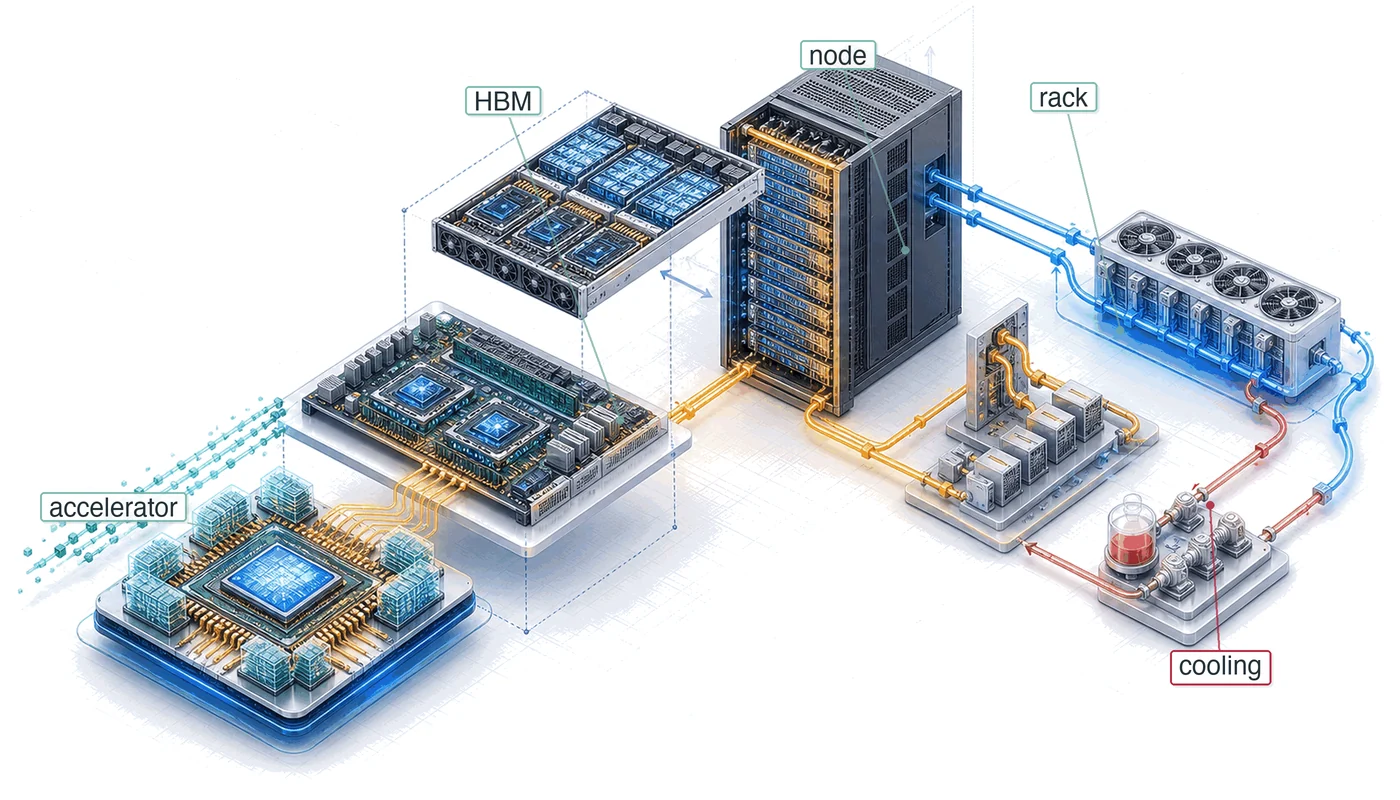
The Infrastructure Walls
Compute Infrastructure
Purpose
Why does infrastructure, not algorithms alone, determine who can participate in advancing machine learning at scale?
Machine learning systems have a physical reality that transcends code. While the algorithms for training large models may be public, the ability to execute them at scale is gated by the physics of infrastructure. Every training run is a race against thermal limits, power delivery stability, and the cost of data movement. When algorithms are the primary bottleneck, progress can happen anywhere. At large scale, the constraint shifts toward who can build and operate the physical systems that make scale possible. Building an ML fleet requires engineering across four physical levels: the accelerator (silicon physics), the node (interconnect density), the rack (thermal management), and the pod (warehouse-scale networking). At each level, the goal is the same: to minimize the time data spends in transit and maximize the time it spends in computation. The economics are equally unforgiving: a large accelerator cluster represents major capital expenditure and megawatts of continuous power. Infrastructure becomes a participation boundary for organizations working at the largest scales. This chapter maps that physical stack, from the stacking of memory dies to the stabilization of grid-scale power ramps. In C³ terms, this substrate is where the fleet’s limits originate: every bound on compute and communication in the chapters that follow traces back to it.
Learning Objectives
- Compare GPU, TPU, and ASIC dataflows to explain specialization across the accelerator spectrum
- Apply roofline analysis to identify compute-, memory-, or bandwidth-bound limits for training and inference
- Calculate token latency or memory budgets from HBM capacity, bandwidth, precision, and model state size
- Map tensor, pipeline, and data parallelism onto NVLink, rack, and pod bandwidth tiers
- Evaluate rack and pod designs using power density, cooling limits, topology, and facility reliability constraints
- Select accelerator infrastructure using sustained throughput, utilization threshold, energy cost, and fleet ownership cost
Scale forces distribution: Compute, Communication, and Coordination replace the single-machine instincts of Data, Algorithm, and Machine. Those fleet-level limits now have to be paid for in hardware. Four physical constraints recur as the system grows from one accelerator to a warehouse-scale pod: memory bandwidth, power delivery, communication bandwidth, and reliability. Figure 1 shows where each wall becomes dominant along that path.
The physical stack begins at the silicon die and expands outward through four levels. At each level, the same engineering pattern appears: a constraint becomes intolerable, and the solution creates the next layer of infrastructure. Nodes aggregate accelerators to overcome memory capacity limits. Racks concentrate nodes and confront power delivery and cooling. Pods wire racks into a warehouse-scale computer and face the communication wall at full force. The path from transistor to data center is anchored by the 175B model, which serves as the thread connecting each level.

Accelerator Spectrum
The foundation starts with the silicon, where a specialized chip earns its place by doing one thing a general-purpose processor cannot do efficiently: run the same dense arithmetic, over and over, at maximum throughput. Consider what happens when a CPU executes a matrix multiplication. The processor fetches an instruction, decodes it, checks for data hazards, routes operands through a deep pipeline, and writes the result back to a register file. For each multiply-accumulate operation, the chip expends energy on branch prediction, speculative execution, out-of-order scheduling, and cache coherence.
These mechanisms exist because a CPU must handle any instruction sequence efficiently, from pointer-chasing linked-list traversals to system calls. For neural network workloads, however, the operation is almost always the same: multiply two matrices of known dimensions, add a bias, and apply a nonlinear function. The CPU’s elaborate control logic represents a tax on every operation, one that buys flexibility the workload does not need. This concept mirrors the classic reduced instruction set computer (RISC) vs. complex instruction set computer (CISC) debate in computer architecture: just as RISC processors achieved higher throughput by simplifying the instruction set, ML accelerators achieve higher throughput by simplifying the computational model to match the dominant workload pattern.
Systems Perspective 1.1: The generality tax
A modern server CPU devotes roughly 30–40 percent of its die area to caches, 20–30 percent to control logic (branch predictors, reorder buffers, instruction decoders), and only 5–10 percent to arithmetic units. This allocation makes sense for general-purpose code, where branches are unpredictable and data access patterns are irregular. For matrix multiplication, however, the access pattern is perfectly regular and the control flow is trivially predictable. Every transistor spent on branch prediction or speculative execution is a transistor that could have been a multiplier. This is the generality tax (principle 5): the silicon area that a processor wastes on capabilities irrelevant to the dominant workload.
The accelerator revolution is, at its core, an exercise in eliminating this tax. Each step along the spectrum from CPU to custom ASIC reclaims more die area for arithmetic by removing another layer of general-purpose control logic. The progression is quantifiable: a CPU devotes roughly 5–10 percent of its die to arithmetic, a GPU devotes roughly 50–60 percent, a Tensor Processing Unit (TPU) devotes roughly 70–80 percent, and a purpose-built ASIC can devote over 90 percent of its die to the target computation.
The transition from general-purpose to specialized silicon follows a logical progression. At one end of the spectrum, GPUs retain substantial programmability while providing 10–100\(\times\) the matrix throughput of CPUs. At the other end, custom ASICs hardwire a specific dataflow for maximum efficiency at the cost of flexibility.
Understanding where each architecture falls on this spectrum, and why, is essential for selecting hardware that matches a given workload. The spectrum is not a ranking from “bad” (general-purpose CPU) to “good” (custom ASIC), but a continuum of trade-offs where each position offers the best match for a different combination of workload characteristics and deployment constraints.
GPUs represent the first major step away from general-purpose computing toward massive parallelism while retaining programmability. An NVIDIA H100, for example, contains 16,896 CUDA cores organized into 132 Streaming Multiprocessors (SMs). Each SM can execute thousands of threads simultaneously using the Single Instruction, Multiple Threads (SIMT)1 execution model. Unlike a CPU, which optimizes for single-thread latency, a GPU hides memory latency by maintaining thousands of threads in flight and switching between them when one stalls on a memory access.
1 SIMT (Single Instruction, Multiple Thread): Coined by NVIDIA to distinguish their GPU model from classical single instruction, multiple data (SIMD). In SIMT, 32 threads form a warp that shares an instruction stream but can diverge at branches; divergence forces serial execution of both paths, halving throughput per branch. For ML workloads, where matrix operations have uniform control flow, warp divergence is rare, which is why GPUs achieve near-peak utilization on general matrix multiply (GEMM) operations but degrade on irregular operations like sparse attention or dynamic routing.
The programmer writes a single function (a kernel), and the hardware maps it across a massive grid of threads. This model is flexible enough to run any mathematical kernel, from convolutions to attention mechanisms to custom loss functions, while providing orders of magnitude more throughput than a CPU for data-parallel computation.
The trade-off is that irregular, branch-heavy code runs poorly because divergent threads within a warp (a group of 32 threads that execute in lockstep) must execute serially. When threads in the same warp take different branches of an if-else statement, the hardware must execute both branches sequentially, disabling the threads that took the other path during each branch. For ML workloads, this divergence penalty is usually small because neural network operations have highly uniform control flow: every element in a matrix multiplication follows the same computation path.
TPUs go a step further, sacrificing some programmability for maximum efficiency on a single operation type by hardwiring the dataflow itself. Google’s Tensor Processing Units use a systolic array2 architecture: a fixed grid of multiply-accumulate (MAC) units where data flows between neighboring cells in a regular, wave-like pattern. Instead of fetching and decoding instructions for each operation, the systolic array receives a matrix at one edge and pulses it through the grid, with each cell performing one MAC and passing the result to its neighbor. This eliminates the instruction fetch and decode overhead entirely, and it avoids writing intermediate results to memory because each partial sum flows directly to the next computation.
2 Systolic Array: From Greek systole (contraction), the systolic-array model was introduced by H. T. Kung and Charles E. Leiserson’s VLSI work and later framed by Kung as a class of architectures where data pulses through a grid of processing elements in a heart-like rhythm (Kung and Leiserson 1979; Kung 1982). The metaphor explains the design: each cell performs one MAC and passes the result to its neighbor, eliminating register-file round-trips. Google’s TPU v1 deployed a \(256{\times}256\) array (65,536 MACs), achieving 92 TOPS within 75 W by hardwiring this dataflow – the architectural bet that made data center-scale inference economically viable (Jouppi et al. 2017).
Kung, Hsiang Tsung, and Charles E Leiserson. 1979. “Systolic Arrays (for VLSI).” Sparse Matrix Proceedings 1978 1: 256–82.
Kung, H. T. 1982. “Why Systolic Architectures?” Computer 15 (1): 37–46. https://doi.org/10.1109/mc.1982.1653825.
Jouppi, Norman P., Cliff Young, Nishant Patil, David Patterson, Gaurav Agrawal, Raminder Bajwa, Sarah Bates, et al. 2017. “In-Datacenter Performance Analysis of a Tensor Processing Unit.” Proceedings of the 44th Annual International Symposium on Computer Architecture, ISCA ’17, 1–12. https://doi.org/10.1145/3079856.3080246.
The cost of this efficiency is reduced programmability. Models must be compiled through Accelerated Linear Algebra (XLA), which maps high-level operations onto the fixed dataflow. Workloads with irregular control flow or dynamic shapes may not map well to this architecture, and the compilation process itself can be time-consuming (minutes to hours for complex models), which slows the iteration cycle during model development.
The programming model distinction between GPUs and TPUs has practical implications for organizational decisions. Research teams that frequently modify model architectures (adding custom attention patterns, experimenting with new activation functions, prototyping novel training algorithms) generally prefer the GPU’s CUDA ecosystem because new operations can be implemented as custom kernels without waiting for compiler support. Teams running established architectures at scale (standard Transformer training, large-scale fine-tuning) may prefer TPUs because the XLA compiler can optimize the entire computation graph, often achieving better hardware utilization than hand-written CUDA kernels for standard operations.
Example 1.1: The TPU origin story
Context: In 2013, Google engineers projected that if users spoke to their Android phones for just three minutes per day using voice search, the company would need to double its data center compute capacity to handle the inference load (Jouppi et al. 2017). The cost was prohibitive.
Insight: Google’s TPU analysis framed production neural-network inference as a dense-linear-algebra workload large enough that voice-search growth alone could have doubled serving capacity needs. This finding led directly to the TPU v1, a purpose-built inference accelerator with a \(256{\times}256\) systolic array that could deliver 92 TOPS (INT8) within a 75 W power envelope. The first TPUs were deployed in 2015 and served production inference workloads including RankBrain and portions of Google Neural Machine Translation (Jouppi et al. 2017); the AlphaGo match-play system is documented separately (Silver et al. 2016).
Systems lesson: Specialization became economically justified because the workload was stable, massive, and dominated by one operation class. The TPU story is a generality-tax case, not merely a faster-chip story.
Silver, David, Aja Huang, Chris J. Maddison, Arthur Guez, Laurent Sifre, George van den Driessche, Julian Schrittwieser, et al. 2016. “Mastering the Game of Go with Deep Neural Networks and Tree Search.” Nature 529 (7587): 484–89. https://doi.org/10.1038/nature16961.
Custom ASICs represent the extreme end of the spectrum, where the economics of silicon justify abandoning general-purpose programmability entirely. When an organization runs a single model architecture at enormous scale, designing a chip specifically for that workload becomes economically rational. By stripping away every feature not required by the target computation, custom ASICs achieve the lowest energy per operation and the highest sustained utilization of any architecture on the spectrum.
Tesla’s Dojo D1 chip, for example, is optimized for the spatial and temporal structure of video-based vision models. Its hundreds of tightly coupled processing nodes are designed around the dataflow needs of Tesla’s vision pipeline, with on-chip SRAM sized to keep spatial tiles close to the compute units. This reduces the repeated round-trips to off-chip memory that a general-purpose GPU would require for the same computation.
AWS Trainium takes a different approach, targeting the broad category of Transformer training rather than a single model. Trainium systems combine compiler-managed memory scheduling with hardware-assisted collective communication, so common training patterns such as tensor-parallel synchronization and data-parallel reductions can be optimized in the accelerator fabric rather than handled entirely by host software.
The risk of custom silicon is equally clear: if the dominant model architecture shifts, as it did from convolutional neural networks (CNNs) to Transformers between 2017 and 2020, a custom ASIC designed for the old architecture becomes a stranded asset. The design cycle for a new ASIC is 2–3 years from conception to deployment, which means the architecture decision must anticipate workload trends several years into the future. This prediction challenge is nontrivial: in 2015, few would have predicted that attention-based Transformers would replace CNNs as the dominant architecture within five years, and organizations that committed to CNN-optimized ASICs during that period found their hardware stranded by the architectural shift.
Custom silicon is therefore a bet on workload stability, and the organizations that make this bet are typically those with enough scale to justify the $50–$200 million development cost and enough workload volume to amortize the per-chip NRE (nonrecurring engineering) cost across millions of chips. Google can justify the TPU’s development cost because high-volume services such as Search, YouTube recommendations, and Gmail spam filtering can amortize a shared accelerator platform. A research lab running a few hundred GPUs cannot justify the same investment.
The bet pays off handsomely when workloads are stable: a purpose-built ASIC can deliver 5–10\(\times\) the energy efficiency of a general-purpose GPU for its target operation. However, the consequences of a wrong bet are severe, as the chip’s fixed dataflow cannot be reprogrammed to accommodate a fundamentally new computational pattern. Pushing the locality argument further leads to a deeper question of physical scale: whether a single die can be expanded to the size of the entire wafer.
Wafer-scale engines
Wafer-Scale Engines (WSE) represent the ultimate pursuit of data locality. While every other architecture on the spectrum relies on chiplets or discrete dies connected by relatively slow PCB-level or package-level interconnects, a wafer-scale engine (like the Cerebras WSE-3) is a single, continuous piece of silicon the size of a dinner plate. By avoiding the need to “dice” the wafer into individual chips, a WSE can maintain a single, massive on-chip interconnect across its entire surface.
The WSE-3 contains 900,000 AI-optimized cores and 44 GB of on-chip SRAM, all connected by a silicon fabric that delivers 21 PB/s of memory bandwidth. To put this in perspective, a single WSE-3 has compute comparable to a large multi-H100 cluster and on-chip memory bandwidth comparable to thousands of H100 HBM links, but because the entire system resides on a single piece of silicon, the communication latency between any two cores is measured in nanoseconds rather than microseconds.
As figure 2 shows, the challenge of wafer-scale integration is physical: manufacturing yield, power delivery, and thermal expansion. A single defect on a standard chip might render it useless, but on a wafer-scale engine, the software must be “defect-aware,” routing around local manufacturing flaws in the silicon fabric. Delivering 23 kW of power to a single piece of silicon and cooling it requires specialized manifold-level liquid cooling that is closer to industrial plumbing than traditional computer engineering.
Wafer-scale engines sit at a unique point on the spectrum: they are highly specialized in their physical architecture but flexible in their computational model, as the underlying cores are often general-purpose enough to execute diverse ML kernels. They represent a “Scale Up” philosophy that attempts to eliminate the communication wall by making the cluster the chip.

The key wafer-scale trade-off is manufacturing complexity and defect-aware routing in exchange for eliminating the inter-chip communication bottleneck entirely, keeping all 900,000 cores within nanoseconds of each other on a single silicon fabric. Figure 3 places these architectures on a continuum, revealing the fundamental trade-off between programmability and efficiency that governs every accelerator design choice. Table 1 turns the same continuum into the architectural features an engineer must compare.

| Feature | CPU | GPU (H100) | TPU (v5p) | Wafer-Scale | Custom ASIC |
|---|---|---|---|---|---|
| Arithmetic Core | Scalar/Vector | Tensor Core | systolic array | RISC-style Core | Fixed Dataflow |
| Execution | Instruction | SIMT | Data-Driven | Dataflow | Hardwired |
| Memory Control | Cache | L1/L2 + HBM | Scratchpad | On-Chip SRAM | Explicit Mesh |
| Flexibility | Extreme | High | Moderate | High | Low |
| Efficiency | Low | High | Very High | High | Extreme |
As table 1 summarizes, for our 175B model, the choice is not purely about peak FLOP/s. If we are a research lab experimenting with novel architectures weekly, the GPU’s flexibility justifies its generality tax. If we are deploying a fixed Transformer at scale for years, the TPU’s dataflow efficiency or a custom ASIC’s power advantage may dominate total cost. The accelerator spectrum is ultimately an economic question of how much flexibility can be surrendered, given the stability of the workload.
Chiplet-based accelerators
A major accelerator design pattern is the chiplet architecture, exemplified by NVIDIA’s Blackwell and AMD’s Instinct MI300 series. Rather than fabricating a single monolithic die, chiplet-based designs partition the processor into multiple smaller dies connected by a high-bandwidth die-to-die interconnect on a common package substrate. This approach addresses two physical limitations that constrain monolithic designs.
First, the maximum die size is capped by the photolithographic reticle limit (the 858 mm² single-exposure ceiling examined in section 1.1.3), which limits the number of Tensor Cores, SMs, and HBM stacks a monolithic GPU can integrate. Chiplet designs bypass this limit by placing multiple dies on a single package, with the B200’s dual-die design effectively creating a 1,600 mm² equivalent processor.
Second, manufacturing yield decreases exponentially with die area because a single defect anywhere on the die renders the entire chip unusable. Smaller chiplets have higher individual yield, and the package-level integration allows partial yields (a defective chiplet can be replaced with a good one). This yield advantage translates directly to lower manufacturing cost per unit of compute, which is particularly important as transistor densities continue to increase and process nodes become more expensive.
The trade-off is the die-to-die interconnect. Communication between chiplets within a package is faster than communication between packages (NVLink) but slower than communication within a single monolithic die (the on-die mesh network). Workloads that generate frequent, fine-grained communication between processing elements (such as operations that share data between nonadjacent SMs) may experience a latency penalty when those SMs reside on different chiplets. GPU vendors mitigate this by making the die-to-die link transparent to the programmer, so the software sees a single logical GPU regardless of the underlying chiplet topology.
Evolution of GPU architectures
The rapid evolution of NVIDIA’s GPU architectures over the past decade illustrates how accelerator design has adapted to the changing demands of ML workloads. Each generation has introduced architectural innovations targeted at the specific bottlenecks revealed by production ML workloads, rather than simply increasing transistor counts.
The Volta architecture (2017) introduced the first-generation Tensor Core, recognizing that neural network training spends the majority of its time in matrix multiplications. By adding dedicated matrix-multiply-accumulate (MMA) hardware alongside the existing CUDA cores, Volta could accelerate the dominant workload pattern without sacrificing the general-purpose programmability that made GPUs attractive for research. The V100, Volta’s flagship, delivered 125 TFLOP/s of FP16 Tensor Core throughput at 300 W.
The Ampere architecture (2020) expanded Tensor Core support to additional data types (TF32, BF16, INT8, INT4), reflecting the growing importance of mixed-precision training and quantized inference. The A100 also introduced Multi-Instance GPU (MIG), which partitions a single GPU into up to seven isolated instances, enabling efficient sharing of expensive hardware across multiple inference workloads. The most consequential change for infrastructure was Ampere’s third-generation NVLink, which doubled bidirectional bandwidth to 600 GB/s per GPU from Volta’s 300 GB/s, directly addressing the communication wall for tensor parallelism, which splits each layer’s matrices across GPUs.
The Hopper architecture (2022) added the Transformer Engine, which dynamically selects between FP8 and FP16 precision on a per-layer basis, doubling the effective throughput for Transformer models without requiring manual precision tuning. Hopper also introduced NVLink 4.0 at 900 GB/s per GPU and the NVLink Switch, enabling NVLink connectivity beyond the 8-GPU boundary.
The H100’s 1979 TFLOP/s of FP8 Tensor Core throughput at 700 W represents a 6.8\(\times\) efficiency improvement over V100, achieved through a combination of process technology (TSMC 4N), architectural innovation (Transformer Engine), and precision engineering (FP8 support).
The Blackwell architecture (2024) continued this trajectory with the B200, which pairs two GPU dies in a single package via a high-bandwidth chip-to-chip link, effectively creating a “dual-die GPU” that delivers about 4,500 TFLOP/s of dense FP8 Tensor Core throughput at 1000 W. FP16/BF16 comparisons should use the lower precision-specific vendor figure rather than the FP8 peak.
The dual-die approach acknowledges that single-die GPU sizes are approaching the reticle limit of lithographic equipment, and further scaling requires chiplet-based designs. The reticle limit is a fundamental constraint of photolithography: the lens system in the EUV scanner can only project a pattern onto an area of approximately \(26{\times}33\) mm (858 mm²) in a single exposure. A die larger than this area would require multiple exposures with stitching, which is technically possible but dramatically increases cost and reduces yield.
Blackwell also introduced fifth-generation NVLink at 1800 GB/s per GPU, doubling the intra-node bandwidth again. The die-to-die link within the B200 package operates at 10 TB/s, fast enough that the two dies can appear as a single logical GPU to the software for many operations.
The progression reveals a consistent pattern: each generation addresses a bottleneck exposed by the previous generation. Volta added dedicated matrix hardware for the compute bottleneck. Ampere expanded mixed-precision support. Hopper targeted Transformer-specific precision with FP8. Blackwell pushed against the die-size limit with multi-die packaging.
At each step, the accelerator’s design reflects an important workload of its era, illustrating how the physics of the workload drives the physics of the silicon. This co-evolution between workloads and hardware is not accidental: accelerator architects profile ML workloads to identify bottlenecks, and then design subsequent generations to address them. The result is a hardware evolution that is tightly coupled to model architecture evolution, which is why Transformer workloads have strongly shaped accelerator design since 2017.
The evolution also reveals a sobering procurement pattern for infrastructure planners: high-end accelerator generations can turn over faster than the facility that houses them. The V100 remained the flagship training GPU for approximately three years (2017–2020). The A100 held that position for roughly two years (2020–2022). Hopper and Blackwell continued that short-cadence pattern in the mid-2020s.
The planning implication is that a data center built for accelerators must anticipate refresh cycles before the first rack arrives. Hardware refresh planning is therefore an integral part of the initial procurement decision, not an afterthought. Table 2 compresses that cadence into the major NVIDIA GPU generations and the interconnect and power changes that arrived with them.
A subtlety that affects fleet consistency is the silicon lottery – the manufacturing reality where microscopic variance in 4nm lithography produces a distribution of chip quality across each wafer. NVIDIA manages this yield curve through aggressive binning: dies capable of sustaining high clock frequencies at strictly controlled voltages under the full TDP are designated as premium H100 SXM modules, while those with higher leakage currents or minor defects become H100 PCIe cards or are fused down to lower-tier products. Even within the top-tier SXM bin, the achievable boost clock varies based on silicon characteristics. In a synchronous training cluster, the collective communication primitives are blocked by the slowest participant. A single chip running 50 MHz below the fleet average can degrade the effective throughput of the entire cluster by 5–10 percent, which is why sophisticated fleet management systems track per-GPU performance metrics and quarantine underperforming silicon to inference pools where the impact of individual chip variance is less pronounced.
| Architecture | Year | Key Innovation | Peak Tensor | TDP | NVLink BW |
|---|---|---|---|---|---|
| Volta (V100) | 2017 | First Tensor Core | 125 TFLOP/s | 300 W | 300 GB/s |
| Ampere (A100) | 2020 | Multi-precision, MIG | 312 TFLOP/s | 400 W | 600 GB/s |
| Hopper (H100) | 2022 | Transformer Engine, FP8 | 1979 TFLOP/s | 700 W | 900 GB/s |
| Blackwell (B200) | 2024 | Dual-die, NVLink 5 | 4,500 TFLOP/s FP8 | 1000 W | 1,800 GB/s |
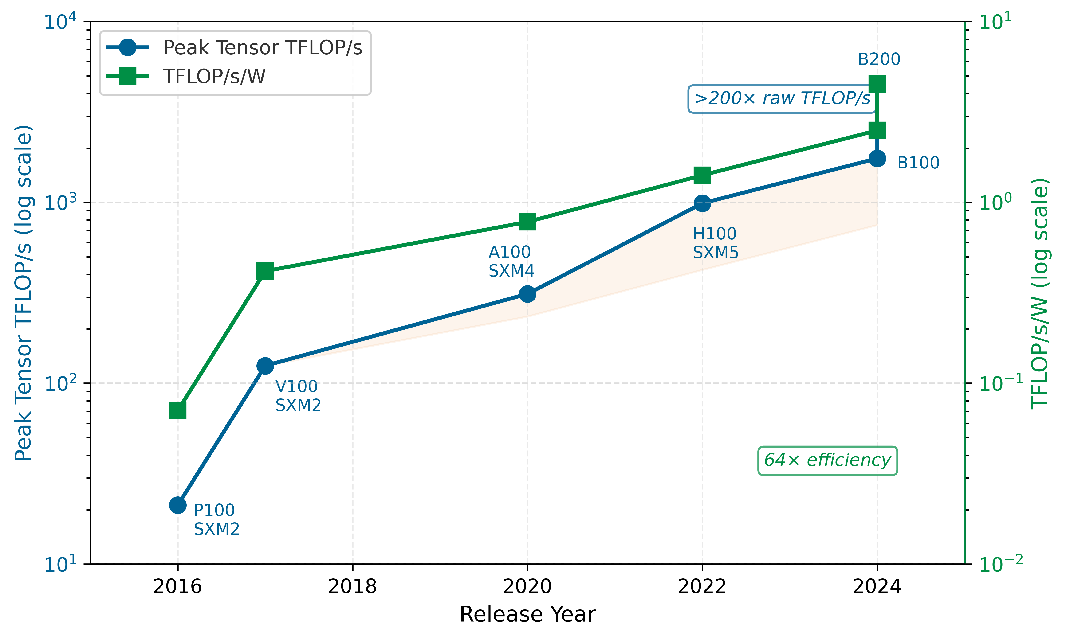
Table 2 compresses four hardware generations into a few columns. Figure 4 unpacks two of those columns, raw throughput and power efficiency, to reveal a divergence that shapes fleet-scale infrastructure decisions.
Figure 4 quantifies a critical asymmetry: while each GPU generation delivers dramatically more raw throughput, the power required to sustain that throughput grows nearly as fast. The advertised low-precision Tensor Core peak from P100 to B200 has grown by more than 200\(\times\), while TFLOP/s per watt has grown far less. The precision modes differ across generations, but that is itself part of the hardware trend: each generation gains compute density partly by introducing lower-precision formats. This divergence is the physical root of the power wall discussed in the next sections and explains why liquid cooling, megawatt-scale power delivery, and thermal management dominate dense accelerator facility design.
Evolution of TPU architectures
Google’s TPU trajectory follows a different path, focusing on distributed efficiency and XLA compiler integration. While GPUs emphasize peak per-chip throughput and software flexibility (CUDA), the TPU is designed from the beginning as a “Pod-scale” resource. Every TPU chip is born as part of a larger cluster, with dedicated inter-chip interconnect (ICI) links that bypass the host CPU entirely.
The generation sequence shows how that pod-first design moved from inference to training. The TPU v1 (2015) was a dedicated inference chip with a \(256{\times}256\) systolic array, delivering 92 TOPS (INT8) for the matrix operations that dominated Google’s production inference workloads. TPU v2 (2017) and TPU v3 (2018) then shifted the architecture toward training by adding bfloat16 (BF16), avoiding the dynamic range problems of standard FP16, and scaling the pod concept to 1,024 chips and 100+ PFLOP/s of aggregate compute. TPU v4 (2021) extended the same logic into the network itself, adding an optical circuit switch (OCS) so the physical topology could be reconfigured for different workloads while raising per-chip BF16 throughput to 275 TFLOP/s.
The TPU v5p (2023) continued this pod-scale design for high-end training. It features 459 TFLOP/s of BF16 compute, 95 GB of HBM2e with 2,760 GB/s memory bandwidth, and 1,200 GB/s bidirectional ICI bandwidth per chip, optimized for the massive AllReduce operations required by billion-parameter models. Table 3 shows how that pod-first design evolved across TPU generations. AllReduce develops the collective communication complexity model and the algorithm choices behind AllReduce, which explain why inter-chip bandwidth, not per-chip arithmetic, sets the ceiling on training throughput as model size grows.
| Generation | Year | Key Innovation | Peak BF16 | HBM | ICI BW |
|---|---|---|---|---|---|
| TPU v1 | 2015 | systolic array (Inference) | 92 TOPS* | — | — |
| TPU v2 | 2017 | High-Bandwidth Memory | 45 TFLOP/s | 16 GB | 600 GB/s |
| TPU v3 | 2018 | Liquid Cooling, Pod Scale | 105 TFLOP/s | 32 GB | 650 GB/s |
| TPU v4 | 2021 | Optical Circuit Switching | 275 TFLOP/s | 32 GB | 1,200 GB/s |
| TPU v5p | 2023 | SparseCore, HBM2e | 459 TFLOP/s | 95 GB | 1,200 GB/s |
As table 3 illustrates, this comparison reveals a divergence in philosophy. GPU evolution is a race to pack more arithmetic and higher-precision Tensor Cores onto a single package, using chiplets (Blackwell) to overcome physical die-size limits. TPU evolution is a race to build more efficient warehouse-scale computers, where the individual chip’s performance is secondary to the pod’s collective bandwidth and reconfigurability (Barroso et al. 2019).
The accelerator’s arithmetic engine performs nearly 2,000 TFLOP/s on the H100. Yet raw arithmetic throughput is meaningless if the data cannot reach the compute units fast enough. The fundamental bottleneck that limits every accelerator’s effective performance is the memory wall.
Self-Check: Question
Order the following processor architectures from highest general-purpose programmability (highest generality tax) to highest operational efficiency (lowest generality tax): (1) Google’s TPU with a systolic array, (2) Tesla’s Dojo custom ASIC, (3) Modern server CPU, (4) NVIDIA GPU with SIMT execution.
A research lab frequently modifies model architectures with custom attention patterns, while a product team runs a fixed, billion-parameter standard Transformer for large-scale fine-tuning. Explain the systems trade-off between choosing GPUs and TPUs for these two teams.
A hardware vendor decides to transition their next-generation accelerator from a monolithic \(800 \text{ mm}^2\) die to a dual-die chiplet architecture connected on a single package. What physical constraint is this transition primarily designed to bypass, and what new bottleneck it introduce?
- It bypasses the communication wall by moving all memory on-chip, but introduces warp divergence because threads must synchronize across the die boundary.
- It bypasses the maximum TDP limit of a single package by separating the thermal loads, but introduces a programming model complexity where developers must write separate kernels for each chiplet.
- It bypasses the reticle limit of EUV lithography equipment and improves manufacturing yield, but introduces a die-to-die interconnect that is slower than an on-die mesh.
- It bypasses the memory wall by doubling the HBM bandwidth per die, but introduces a generality tax because each chiplet needs its own control logic.
Why does a Wafer-Scale Engine (WSE) require “defect-aware” routing software, whereas a cluster of traditional monolithic GPUs does not?
- A WSE eliminates the need for liquid cooling, so the silicon experiences higher thermal variance that creates temporary dynamic defects during computation.
- A WSE uses a single continuous piece of silicon where manufacturing flaws cannot be physically discarded by dicing, so the software must route around local defects in the fabric.
- A WSE connects 900,000 cores using standard Ethernet protocols, which natively drop packets and require software-level retry mechanisms.
- A WSE compiles standard PyTorch models into a fixed dataflow that naturally introduces algorithmic defects during the XLA lowering process.
True or False: From the P100 to the B200 generation, NVIDIA GPUs have increased their power efficiency (TFLOP/s per watt) at roughly the same rate as their peak raw throughput (TFLOP/s).
The Memory Wall
With the accelerator’s arithmetic engine selected, we confront a paradox: the faster we make our logic, the more it idles waiting for data. This diverging trajectory between processor throughput and data access speed is formally known as the Memory Wall (Wulf and McKee 1995). While transistor scaling has driven logic performance up by orders of magnitude, the physical interconnects that feed data to these cores have failed to keep pace. This bottleneck is existential for machine learning: unlike traditional software that benefits heavily from caching and data reuse, neural networks must stream billions of weights from memory for every inference pass, often making bandwidth – not compute – the governing constraint on performance. Diagnostic Summary develops the diagnostic framework that classifies this memory-bound condition alongside the other bottleneck patterns a fleet encounters, so that a measured symptom maps to a named constraint rather than a guess.
Wulf, Wm. A., and Sally A. McKee. 1995. “Hitting the Memory Wall: Implications of the Obvious.” ACM SIGARCH Computer Architecture News 23 (1): 20–24. https://doi.org/10.1145/216585.216588.
The implications are concrete and perceptible in our running example. Our 175B model’s weights occupy 350 GB in FP16. During autoregressive decoding, this entire 350 GB tensor must be streamed from off-chip memory into the processor’s registers for every single token generated. A single H100 cannot hold that tensor, so this is a bandwidth-floor calculation after sharding or quantization has solved the capacity problem. At H100-class HBM bandwidths (~3.35 TB/s per accelerator), the data movement alone dictates a latency floor of over 100 ms per token if one accelerator-equivalent bandwidth path must stream the weights. The memory wall is not an abstract architectural concept: it is the physical reason a chatbot takes a perceptible pause between words. Three engineering responses address this constraint: high bandwidth memory (HBM) widens the data pipe, the roofline model rigorously diagnoses whether a workload is starving for data or for compute, and Tensor Cores maximize the arithmetic value of every byte fetched. As figure 5 shows, memory bandwidth is also a placement trade-off: moving the working set closer to compute raises bandwidth, but it usually reduces the amount of state that can stay there.
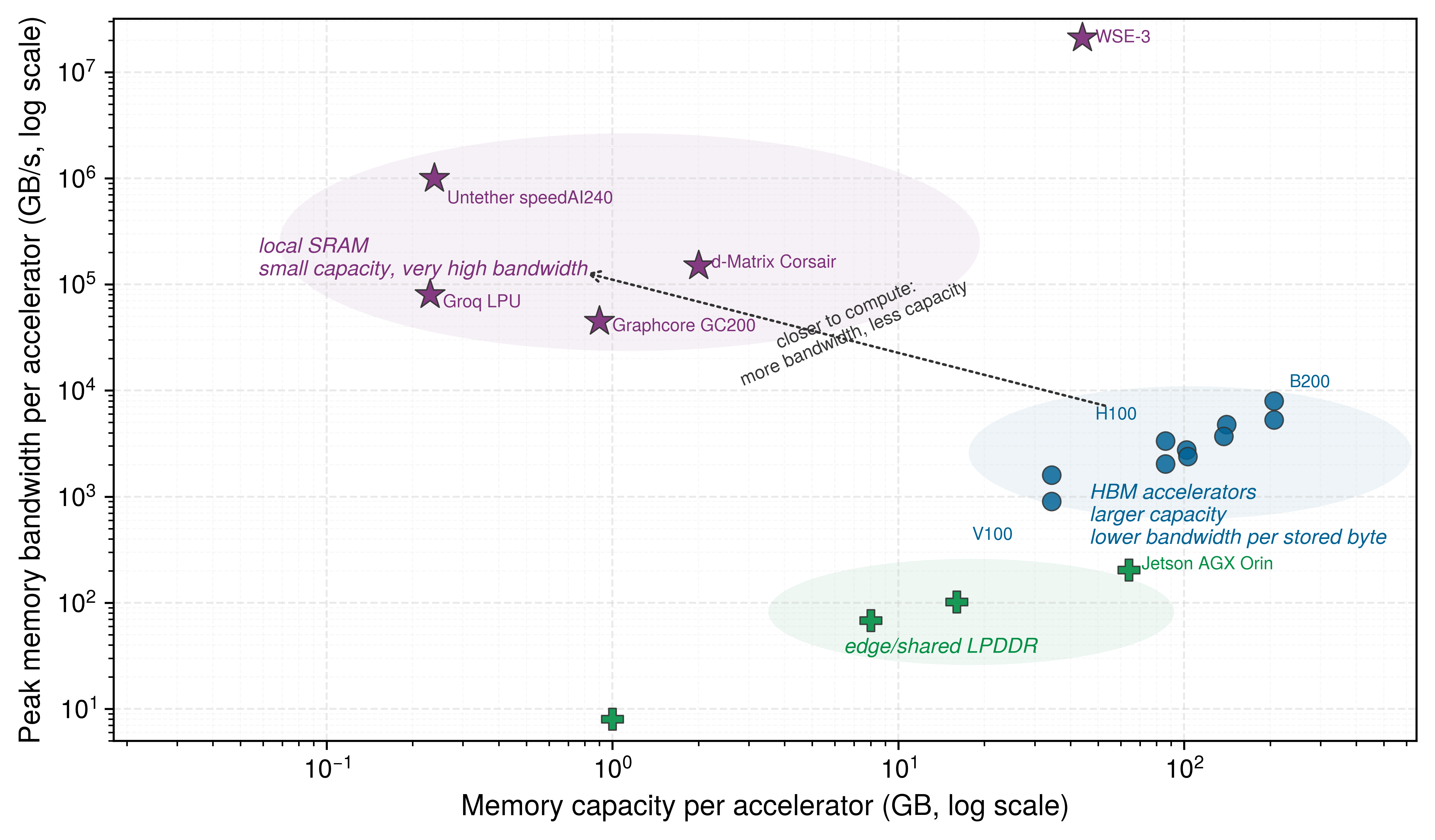
Figure 5 is not a ranking of accelerators; it is a map of where each design chooses to place bytes. Edge devices keep memory cheap and compact, but bandwidth stays low. HBM moves memory onto the accelerator package, buying enough capacity and enough bandwidth for active model state. Local-SRAM designs push the working set still closer to arithmetic, buying extraordinary bandwidth at the cost of much smaller resident capacity. That tier map explains why HBM is the next engineering response: it is not the fastest memory in the system, but it is the highest-bandwidth tier that can hold tens to hundreds of gigabytes next to the compute die.
HBM: Breaking the memory wall
An H100 can execute nearly 2,000 TFLOP/s of low-precision matrix arithmetic, yet during autoregressive decoding of our 175B model, its Tensor Cores would sit idle for over 99 percent of each cycle in a bandwidth-floor model. The bottleneck is not the speed of multiplication but the speed of delivery: once the model has been sharded or compressed so the weights fit, the serving path must still stream the active weight shards through the arithmetic units for every output token. No amount of additional Tensor Cores can help when the existing ones are already starved for data. The accelerator response to this fundamental limitation is High Bandwidth Memory3.
3 HBM (High Bandwidth Memory): Standardized by JEDEC in 2013 as a joint development between AMD and SK Hynix, originally for graphics cards. ML accelerators adopted HBM because neural networks exhibit the same bandwidth-hungry, capacity-moderate access pattern as high-end rendering. Each HBM generation has roughly doubled bandwidth (128 GB/s in HBM1 to 1.2 TB/s per stack in HBM3e), yet the gap between memory bandwidth and arithmetic throughput continues to widen – making HBM a necessary but never sufficient response to the memory wall.
4 Register File Bandwidth: In an H100 GPU, the register file provides over 300 TB/s of aggregate bandwidth to the CUDA cores. This is ~100\(\times\) higher than HBM3 bandwidth, explaining why tiling is mandatory: any operand not in a register during execution forces the arithmetic units to wait 100+ clock cycles for data, collapsing utilization.
5 SRAM Energy (pJ/bit): Accessing a bit in SRAM (shared memory) consumes approximately 0.1–0.5 pJ, while fetching from HBM consumes 2–5 pJ. This 10\(\times\) energy difference is the physical driver behind kernel fusion: every intermediate result kept in SRAM instead of written to HBM saves both time and significant power and thermal headroom.
The memory hierarchy within a single accelerator spans orders of magnitude in both capacity and bandwidth. At the top sits the register file4 – approximately 20–30 MB distributed across all SMs – with effectively infinite bandwidth (hundreds of TB/s) but minuscule capacity. Below this lies the L1 cache and shared memory (SRAM)5, offering roughly 256 KB per SM (approximately 33 MB total) with an aggregate bandwidth of ~19 TB/s. Further down sits the 50 MB L2 cache (~12 TB/s), and finally the 80 GB of HBM3 at 3.35 TB/s.
Lighthouse 1.1: Archetype B (DLRM at Scale): The capacity wall
While Archetype A (GPT-4) is primarily throughput-bound (demanding more TFLOP/s), Archetype B (DLRM at Scale), the DLRM workload, is primarily capacity-bound. A 10 TB embedding table cannot fit into the 80 GB HBM of a single H100, nor can it fit into the aggregate HBM of a single 8-GPU node (640 GB). Capacity alone requires at least 16 such nodes before accounting for replication, hot-table headroom, and bandwidth balance; production-scale recommenders often grow to much larger multi-node shards, transforming a memory-access problem into a massive All-to-All network coordination problem.
The bandwidth gap between registers and HBM is approximately 100\(\times\). If an operand must be fetched from HBM for a single operation, the arithmetic unit spends about 99 percent of its time stalling. High Model FLOPs Utilization (MFU), the fraction of peak hardware FLOP/s spent on useful model computation, is only possible through aggressive tiling: breaking the massive weight matrices into small tiles that fit entirely within shared memory and registers, then performing as many multiply-accumulate operations on each tile as possible before evicting it. As figure 6 illustrates, this strategy loads data once into the SM’s fast SRAM and reuses it across multiple Tensor Core operations, effectively multiplying the arithmetic value of every byte fetched from HBM.

Despite the 175B model’s massive total memory footprint, the active working set at any given microsecond must be meticulously managed to reside in that top 30 MB of register space, or the chip’s theoretical performance becomes a mirage. HBM supplies the bulk capacity, but tiling decides whether that capacity feeds the arithmetic units fast enough to matter.
Definition 1.1: High bandwidth memory (HBM)
High Bandwidth Memory (HBM) is the 3D-stacked DRAM architecture used by ML accelerators, in which multiple memory dies are vertically bonded and connected to the processor through thousands of Through-Silicon Vias (TSVs) on a shared silicon interposer, eliminating the centimeter-scale PCB traces of conventional DRAM and replacing them with micrometer-scale vertical paths.
- Significance: HBM3 in the H100 delivers approximately 3.35 TB/s of memory bandwidth—roughly 16\(\times\) DDR5’s ~200 GB/s—at 2 pJ/bit vs. DDR5’s ~20 pJ/bit. This bandwidth sets the \(\text{BW}\) ceiling in the iron law: the H100’s FP16 ridge point is approximately \(989\,\text{TFLOP/s} / 3.35\,\text{TB/s} \approx 295\) FLOP/byte, so any operator with arithmetic intensity below 295 FLOP/byte (for example, attention at 5–20 FLOP/byte) remains memory-bound even with HBM.
- Distinction: Unlike DDR memory, which connects through centimeters of PCB trace (introducing capacitance, attenuation, and high driving current), HBM uses 1,024-bit-wide TSV buses with path lengths measured in micrometers, a 1,000\(\times\) reduction in signal distance that enables the wider bus without proportionally higher power.
- Common pitfall: A frequent misconception is that HBM solves the memory wall. HBM moves the wall rather than eliminates it: Tensor Core throughput \((R_{\text{peak}})\) has scaled faster than HBM bandwidth across generations (from 900 GB/s with 125 TFLOP/s FP16 in V100 to 3.35 TB/s with 989 TFLOP/s FP16 in H100), so the ridge point continues rising and more operations remain memory-bound despite HBM improvements.
Traditional DDR memory connects to the processor through pins on the edge of a printed circuit board (PCB). Each DIMM communicates over a 64-bit bus, and even with multiple channels (8 channels is typical for a high-end server CPU), a modern server tops out at roughly 200 GB/s of aggregate memory bandwidth.
The physical distance from the DIMM slot to the processor die is measured in centimeters, and every centimeter of copper trace introduces capacitance, signal attenuation, and energy loss. At DDR5 data rates (4,800–6,400 MT/s per pin), the signal conditioning circuits must compensate for significant channel impairment, consuming substantial power per bit transferred. Increasing the data rate on these long traces requires progressively more power for signal conditioning, creating a diminishing-returns curve that DDR5 is already approaching.
HBM solves this problem by changing the physical topology entirely, as figure 7 shows. Instead of routing signals horizontally across a PCB, HBM stacks multiple DRAM dies vertically, one on top of another, and connects them with Through-Silicon Vias (TSVs)6: microscopic copper pillars etched through the silicon substrate itself.
6 TSV (Through-Silicon Via): A vertical copper pillar, 5–10 micrometers in diameter, etched through a silicon die to connect stacked layers. Originally developed for CMOS image sensors in smartphone cameras, TSVs enabled HBM by replacing centimeters of PCB trace with tens of micrometers of vertical silicon—a 1,000\(\times\) reduction in signal path that drops energy per bit from ~20 pJ (DDR5) to ~2 pJ (HBM), making terabyte-per-second bandwidth economically feasible within an accelerator’s power budget.

The vertical stacking represents a fundamental change in memory architecture: rather than increasing bandwidth by pushing signals faster through long copper traces (the DDR approach, which has diminishing returns), HBM increases bandwidth by multiplying the number of parallel signal paths through extremely short vertical connections. A single HBM stack bonds 8–12 DRAM dies vertically, threading thousands of TSVs through each die to form a 1024-bit-wide interface per stack, compared to 64 bits for a DDR5 channel. This 16\(\times\) wider interface, combined with higher per-pin signaling rates, is the source of HBM’s bandwidth advantage. Because the vias travel through the silicon rather than across a PCB, the signal path shrinks from centimeters to tens of micrometers, roughly a 1000\(\times\) reduction, and the whole stack sits on the same silicon interposer as the processor die so data travels from DRAM cell to arithmetic unit in nanoseconds rather than the tens of nanoseconds required by off-package DDR.
The shortened distance has three direct physical benefits:
- Energy per bit: The transfer cost drops by an order of magnitude, from approximately 20 pJ/bit for DDR5 to approximately 2 pJ/bit for HBM, because shorter traces have lower capacitance and require less driving current.
- Latency: Electrical signals propagate through silicon at roughly two thirds the speed of light, so the shorter path reduces propagation time.
- Signaling rate: Lower capacitance allows higher signaling frequencies without the sophisticated equalization circuits required by long PCB traces, enabling the high per-pin data rates that complement the wide bus width.
Together, these effects explain why HBM widens the interface and shortens the path instead of simply driving off-package pins faster.
Checkpoint 1.1: HBM and the memory wall
These questions check whether the physical benefits of 3D-stacked memory are clear:
Table 4 summarizes the physical trade-off: HBM wins bandwidth by moving memory onto the package and widening the interface, not by making each off-package signal faster.
| Metric | Host DRAM (DDR5) | Accelerator HBM (HBM3e) | Scaling Factor |
|---|---|---|---|
| Mechanism | 2D PCB Traces | 3D Die Stacking | - |
| Placement | Socketed DIMMs | On-package (Substrate) | Physical Proximity |
| Bandwidth | ~200 GB/s | ~3.35 TB/s | ~17\(\times\) Faster |
| Interface Width | 64-bit | 1024-bit per stack | 16\(\times\) Wider |
| Energy | ~20 pJ/bit | ~2–5 pJ/bit | 4–10\(\times\) Efficiency |
As table 4 shows, this bandwidth advantage comes at a price. HBM costs approximately $10–15 per GB, compared to roughly $3 per GB for DDR5 server memory. For an H100 with 80 GB of HBM3, the memory alone represents approximately $800–1,200 of the accelerator’s manufacturing cost. For a B200 with 192 GB of HBM3e, the memory cost rises to $1,920–2,880 per accelerator, making HBM one of the most expensive components in the system.
The advanced packaging process, which requires precise alignment of thousands of TSVs across multiple die layers, has lower manufacturing yields and higher complexity. Each step in the stacking process (die thinning, alignment, bonding, and TSV etching) can introduce defects. The cumulative yield across 12 stacking steps means that the overall yield for a complete HBM3e stack is substantially lower than the yield for a single DRAM die. The silicon interposer itself must be large enough to accommodate both the processor die and multiple HBM stacks (often exceeding 1,000 mm² in total area), and any defect in a TSV can render an entire stack unusable.
The supply chain dynamics of HBM production further affect its cost and availability. The HBM supply chain is highly concentrated among a small number of manufacturers, and the production processes (die thinning, TSV etching, die-to-die bonding) require specialized capital equipment that is fundamentally different from standard DRAM manufacturing. Expanding HBM production capacity requires 12–18 months of equipment procurement and qualification, which means that production cannot rapidly scale in response to demand surges. When demand outpaces supply, as it did following the explosion of interest in large language models in 2023, lead times stretch to 12–18 months and prices can double.
For infrastructure planners, this supply chain concentration means that HBM availability, not just its specifications, can determine the timeline for building a training cluster. Organizations planning large deployments must secure HBM allocations 12–18 months in advance, committing capital before the rest of the system is designed. This procurement lead time is longer than for any other component in the stack, making HBM the pacing element for fleet expansion.
For our 175B model, the HBM alone in a cluster of 1,000 accelerators represents roughly $0.8–1.2 million at 80 GB/accelerator (or $2–3 million at 192 GB/accelerator) under the $10–15/GB cost model above. This cost-capacity trade-off explains why accelerators typically offer 80–192 GB of HBM while the host server provides 512 GB to 2 TB of DDR: the fast memory holds the active computation (weights, activations, gradients that are accessed every cycle), and the cheap memory holds everything else (optimizer states, checkpoint buffers, data loading queues).
The boundary between what resides in HBM and what resides in DDR is a critical design parameter for training frameworks, and managing this boundary efficiently is one of the key challenges addressed by ZeRO (Zero Redundancy Optimizer) sharding and offloading strategies described in Memory-efficient data parallelism: ZeRO and FSDP. Sharding divides optimizer, gradient, and parameter state across workers; offloading places colder state in host DRAM or NVMe when HBM capacity is the binding limit. Getting this boundary wrong in either direction is costly: placing too much data in HBM wastes expensive capacity, while placing too much in DDR creates bandwidth stalls that idle the arithmetic units.
HBM generations and the scaling boundary
The evolution of HBM tracks the growth of model sizes with close correspondence. Each generation increases the number of stacked dies, the signaling rate per pin, and the total capacity per stack, driven by the relentless growth in model parameters. Table 5 shows the scaling boundary: HBM4 must widen the interface because pin-rate increases alone are no longer enough.
| Metric | HBM2e (A100) | HBM3 (H100) | HBM3e (B200) | HBM4 (Future) |
|---|---|---|---|---|
| Peak Bandwidth | ~2.0 TB/s | ~3.3 TB/s | ~8.0 TB/s | 12–16 TB/s (projected) |
| Typical Capacity | 40–80 GB | 80–96 GB | 192 GB | 288 GB+ |
| Interface Width | 1024-bit | 1024-bit | 1024-bit | 2048-bit |
| Stack Height | 8 dies | 8–12 dies | 12 dies | 16 dies |
As table 5 shows, the transition from HBM3 to HBM3e is particularly significant for our running example. An A100 with 80 GB of HBM2e can hold only 23 percent of our 175B model’s weights (at FP16). An H100 with 80 GB of HBM3 can hold the same fraction but deliver the data 65 percent faster. A B200 with 192 GB of HBM3e can hold 55 percent of the weights and deliver them at about 8 TB/s. Neither can hold the full model, which is precisely why we need multiple accelerators in a node, a topic we address in section 1.3.
However, the capacity story changes significantly when quantization is applied. The same 175B model quantized to INT8 requires only 175 GB, fitting in 3 H100 GPUs or a single B200. Quantized to INT4, it requires only 87.5 GB, fitting in two H100 GPUs. The capacity constraints that drive the need for multi-accelerator nodes for training (where FP16 or BF16 precision is typically required) are substantially relaxed for inference (where INT8 or INT4 quantization is often acceptable). This is another reason why training and inference infrastructure have different optimal configurations.
The bandwidth improvement matters independently of capacity. Each generation of HBM produces a nearly proportional reduction in per-token latency during autoregressive inference once the capacity problem has been handled by sharding or quantization.
A 70.6B FP16 model has 141 GB of weights, so a bandwidth-floor calculation gives roughly 141 GB/2.04 TB/s = 69.2 ms per token at A100-class bandwidth, 141 GB/3.35 TB/s = 42.1 ms at H100-class bandwidth, and 141 GB/8 TB/s = 17.7 ms at B200-class bandwidth. The A100 and H100 cases do not imply that the full FP16 model fits on one device; they isolate the latency floor imposed by a single accelerator-equivalent HBM path. For interactive applications (chatbots, code assistants, real-time translation), where users perceive delays above 50 ms as “slow,” these bandwidth improvements translate directly into better user experience and into the ability to serve larger models within latency budgets.
The projected jump to HBM4 doubles the interface width from 1024 bits to 2048 bits for the first time since HBM’s introduction. This signals that per-pin signaling rate increases alone cannot sustain bandwidth growth indefinitely, and the bus must widen. The doubling of interface width requires a correspondingly larger interposer area for routing, which is one reason accelerator packages have tended to grow as bandwidth targets rise.
HBM4-class packages projected in the 12–16 TB/s aggregate range illustrate the planning pressure created by trillion-parameter-scale models. A 1T-parameter model requires roughly 2 TB of weight storage in FP16. At B200-class HBM3e bandwidths (about 8 TB/s), serving such a model at batch size 1 would produce tokens at 2000 GB/8 TB/s = 250 ms per token, far too slow for interactive applications. Even at 16 TB/s, the bandwidth floor remains roughly 125 ms per token before batching, quantization, or tensor-parallel sharding. This calculation suggests that trillion-parameter models require aggressive quantization and multi-accelerator tensor parallelism even for single-request inference. The co-evolution of model scale and memory technology continues to drive infrastructure requirements.
An important architectural consideration is the number of HBM stacks per accelerator and how they connect to the processor. The H100 has 5 HBM3 stacks, each providing approximately 670 GB/s, for a total of 3.35 TB/s aggregate bandwidth. A B200-class Blackwell GPU package uses 8 HBM3e stacks for an aggregate of about 8 TB/s. The number of stacks is constrained by the interposer area available for HBM placement: each HBM stack occupies approximately 100 mm² of interposer area, and the total interposer must accommodate both the processor die(s) and all HBM stacks. Larger interposers allow more HBM stacks (and therefore higher bandwidth and capacity) but are more expensive and harder to manufacture.
The interposer area constraint creates a concrete design tension. Making the processor die larger (more Tensor Cores, more SMs) leaves less interposer area for HBM stacks, potentially reducing bandwidth. Making the processor die smaller (fewer Tensor Cores) frees interposer area for more HBM but reduces peak compute throughput. The optimal balance depends on the target workload’s position on the Roofline plot: compute-bound workloads benefit from a larger processor die (more Tensor Cores), while bandwidth-bound workloads benefit from more HBM stacks. The single-accelerator roofline derives the ridge point that separates these two regimes, expressing it through equation and equation so that a workload’s arithmetic intensity predicts which side of the balance it falls on before any silicon is committed.
Memory bandwidth and token latency
The distinction between memory capacity (how many gigabytes the HBM can store) and memory bandwidth (how many terabytes per second it can deliver) is one of the most practically important concepts in ML infrastructure. Capacity determines whether a model’s weights fit. Bandwidth determines how fast the model can run. For autoregressive text generation, where each token requires a full pass through the model’s weights, bandwidth is almost always the binding constraint. The α-β Communication Model formalizes the same latency-versus-bandwidth decomposition for data movement across the network, giving the reader a single algebraic model that applies equally to the memory system here and to inter-node transfers later.
Napkin Math 1.1: The physics of token latency
Problem: Generating one token from Llama-3 70B (141.2 GB of FP16 weights) requires both arithmetic and a full weight load from HBM. Assuming capacity has been solved (by sharding, a higher-capacity device, or quantization), which dominates the per-token time on an H100: compute or memory transfer?
- Compute Time: Each token requires \(2 \times 70 \times 10^9 = 1.4 \times 10^{11}\) floating-point operations. At 989 TFLOP/s of FP16/BF16 Tensor Core peak throughput, the arithmetic takes \(T_{\text{compute}} \approx \mathbf{0.14 \text{ ms}}\).
- Memory Time:
Loading 141.2 GB of weights from HBM at 3.35 TB/s takes \(T_{\text{mem}} \approx \mathbf{42.1 \text{ ms}}\).
Systems insight: The processor spends 99.7 percent of its time waiting for data from memory. The arithmetic units are idle for almost the entire token generation. Even a hypothetical processor with infinite compute throughput would generate tokens only negligibly faster, because the memory transfer time dominates completely. This is why HBM bandwidth improvements deliver nearly linear speedups for inference workloads.
That bandwidth floor also gives us a clean way to compare adjacent hardware generations: if compute stays fixed while HBM capacity and bandwidth improve, decode latency should move with the memory system rather than the arithmetic units.
Napkin Math 1.2: The memory wall: H100 vs. H200
To understand why the “memory wall” is the primary constraint for modern large language models (LLMs), we compare the NVIDIA H100 against its successor, the H200. While both chips share the same compute cores (same peak TFLOP/s), the H200 provides 1.4× higher memory bandwidth and 1.6× more HBM capacity.
This LEGO comparison uses a Llama 3 model with 70.6B parameters, sequence length 2,048, and batch size 1; the reported speedup is the serving solver’s inter-token latency estimate, not a raw bandwidth ratio alone. A napkin estimate brackets that solver number: decode spends 99.7 percent of its per-token time on the weight load, so the expected gain is the HBM bandwidth ratio, 4.8 TB/s \(\div\) 3.35 TB/s \(\approx\) 1.4×.
Systems insight: For LLM decoding, the H200 is 1.4× faster than the H100 despite having identical compute power; the solver’s estimate lands almost exactly on the bandwidth ratio because decode is bandwidth-bound. This proves that for large-scale autoregressive models, the “Wall” is the memory interface, not the arithmetic logic.
The napkin math reveals a profound asymmetry at the heart of modern ML infrastructure. The accelerator vendors invest billions of dollars in designing faster arithmetic units (more Tensor Cores, higher clock speeds, wider datapaths), yet for single-request inference, the arithmetic completes in a fraction of a millisecond while the memory transfer takes tens of milliseconds. The arithmetic units are about 300\(\times\) faster than the memory system for this workload, meaning that over 99 percent of the silicon dedicated to computation is idle during inference. That compute-memory asymmetry is the single most important physical fact about ML inference, and it shapes every architectural and economic decision about serving infrastructure.
The fraction of token time spent waiting on memory, 99.7 percent in this example, is called the memory-boundedness of the workload. A workload that is 99 percent memory-bound will see almost no benefit from a faster processor (more TFLOP/s) but will see nearly linear speedup from faster memory (more TB/s bandwidth).
Memory-boundedness is a quantitative expression of the memory wall: the gap between processing speed and memory speed has widened for decades and is particularly acute for ML inference workloads. The memory wall was first identified by Wulf and McKee in 1995, who observed that processor speed was improving at 60 percent per year while DRAM speed improved at only 7 percent per year. The growing disparity meant that processors would increasingly spend their time waiting for data rather than computing on it. Thirty years later, their prediction has proven accurate, and the ML inference workload is the most extreme manifestation of the memory wall in modern computing.
The practical implication is that accelerator selection for inference workloads should prioritize bandwidth-per-dollar over FLOP/s-per-dollar. An older-generation GPU with high memory bandwidth but moderate compute throughput may deliver better inference performance per dollar than a latest-generation GPU with extreme compute but insufficient bandwidth improvement.
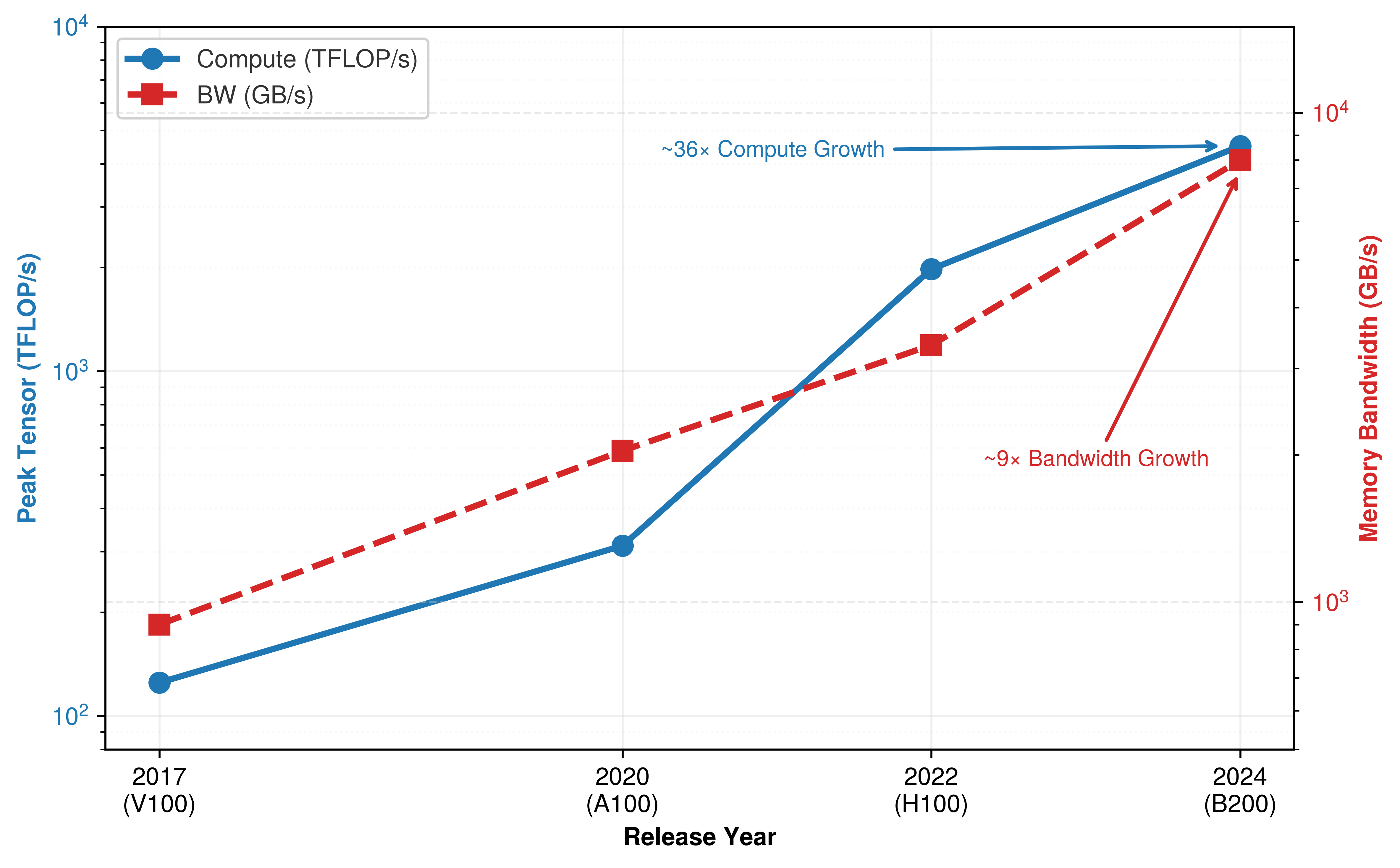
Figure 8 makes this divergence visible across four GPU generations. While peak Tensor throughput has grown 36\(\times\) from V100 to B200 when following each generation’s advertised low-precision mode, memory bandwidth has grown only 9\(\times\) over the same period. The widening gap between compute growth and bandwidth growth is the memory wall: each generation of accelerator becomes more powerful in arithmetic but proportionally more starved for data.
For training workloads, where large batch sizes increase arithmetic intensity, the calculus shifts toward compute: peak TFLOP/s per dollar becomes the relevant metric because the weight data loaded from HBM is amortized across many tokens in the batch. The Roofline Model, which we examine next, provides the formal framework for making this trade-off precise and for determining which metric matters for any given workload.
Roofline model
The token latency calculation above demonstrated that a 70B model on an H100 is overwhelmingly memory-bound. The question is how to determine this systematically for any workload on any hardware. The Roofline Model7, introduced by Williams, Waterman, and Patterson (Williams et al. 2009), provides a visual and analytical framework that answers this question with a single number: the arithmetic intensity of the workload.
7 Roofline Model: Introduced by Williams, Waterman, and Patterson at UC Berkeley in 2009, the model plots attainable FLOP/s against arithmetic intensity on a log-log scale, producing two intersecting lines whose crossover point – the ridge point – separates memory-bound from compute-bound regimes.
Williams, Samuel, Andrew Waterman, and David Patterson. 2009. “Roofline: An Insightful Visual Performance Model for Multicore Architectures.” Communications of the ACM 52 (4): 65–76. https://doi.org/10.1145/1498765.1498785.
For an H100 (989 TFLOP/s FP16, 3.35 TB/s HBM), the ridge point is ~295 FLOP/byte; most LLM inference operators fall well below this threshold, which is why the Roofline remains the first diagnostic tool for identifying whether more compute or more bandwidth will improve performance. The quantity that places a workload on this plot is its arithmetic intensity \((I)\), defined as \(I = \text{FLOP}/\text{byte}\): the ratio of computation to memory traffic that determines whether a workload is bandwidth-bound or compute-bound. The same quantity carries forward to fleet-scale performance analysis at The roofline model.

Decode sits deep in the memory-bound regime, far below the ridge.
The Roofline Model expresses the maximum achievable performance of a workload as the lesser of two ceilings:
\[ \text{Achievable FLOP/s} = \min\left(R_{\text{peak}},\ \text{BW} \times I\right) \tag{1}\]
Equation 1 has a direct physical interpretation. If the workload’s arithmetic intensity is low (it needs many bytes per operation), then performance is limited by how fast memory can deliver those bytes. The achievable FLOP/s grows linearly with \(I\), tracing a sloped line on a log-log plot. If the arithmetic intensity is high (each byte fuels many operations), then performance plateaus at the hardware’s peak compute rate, regardless of further increases in \(I\). This plateau is the flat “roof” of the model.
Definition 1.2: Ridge point
Ridge Point is the ML accelerator arithmetic intensity where the memory bandwidth ceiling meets the compute ceiling \((I_{\text{ridge}} = \frac{R_{\text{peak}}}{\text{BW}})\).
- Significance: It defines the Hardware Efficiency Threshold. Workloads with an intensity below the ridge point are bandwidth-bound \((\text{BW})\), while those above are compute-bound \((R_{\text{peak}})\).
- Distinction: Unlike Peak FLOP/s (which only describes the horizontal ceiling), the ridge point describes the Balance of the architecture. A rising ridge point over hardware generations indicates that compute is growing faster than bandwidth, making utilization harder.
- Common pitfall: A frequent misconception is that all GPUs have the same ridge point. In reality, it varies by Precision: because \(R_{\text{peak}}\) is higher for INT8 than FP32 while \(\text{BW}\) is constant, the ridge point for INT8 is much higher, requiring more data reuse to saturate the hardware.
Specific ML workloads occupy different regions of this plot depending on the operation and the batch size:
- LLM decode (batch size 1): Each token requires loading the full weight tensor (~2 bytes per parameter) for just 2 FLOPs per parameter, yielding \(I \approx 1\) FLOP/byte. This is deep in the memory-bound region, well below the ridge point of 295.2 FLOP/byte. Our token latency calculation confirmed this: the arithmetic finished in microseconds while the memory transfer took milliseconds.
- LLM prefill (large context): Processing a long input sequence in parallel increases the FLOPs (matrix-matrix multiply instead of matrix-vector) without proportionally increasing memory traffic, pushing \(I\) to 100–500 FLOP/byte. This range straddles the H100 ridge point: the lower end remains memory-bound or near the ridge, while the upper end crosses into the compute-bound region.
- CNN training (large batch): Convolution with large spatial dimensions and batch sizes achieves \(I\) of 50–200 FLOP/byte, placing it near or above the ridge point for most accelerators.
- Attention (long sequences): The self-attention mechanism scales quadratically with sequence length in FLOPs but linearly in memory traffic for the KV cache, making its arithmetic intensity sequence-length-dependent. Short sequences are memory-bound; long sequences are compute-bound.
The point is to classify each phase and batch shape on the roofline, not to assign one permanent region to an entire model family.
Reading a Roofline plot requires understanding what each axis represents. The horizontal axis is arithmetic intensity (FLOP/byte), plotted on a log scale. The vertical axis is achievable performance (FLOP/s), also on a log scale. Two lines define the “roofline” shape: a diagonal line with slope 1 (on the log-log plot) representing the memory bandwidth limit, and a horizontal line representing the peak compute limit. These two lines meet at the ridge point.
Any workload can be plotted as a single point on this chart by computing its arithmetic intensity and measuring its achieved performance. If the point lies on the diagonal line, the workload is memory-bound and would benefit from faster memory. If it lies on the horizontal line, the workload is compute bound and would benefit from more arithmetic units.
If the point lies below either line, the workload is not fully using the available resource. This gap indicates an optimization opportunity in the software: kernel inefficiency, poor memory access patterns, or excessive synchronization. Closing this gap is the province of kernel engineering and communication optimization, topics examined in Performance Engineering.
The Roofline’s diagnostic power extends beyond individual kernels to entire training runs. For our 175B model, the computation graph contains thousands of distinct operations with different arithmetic intensities. The dense Feed-Forward Network (FFN) layers are dominated by large GEMMs with high arithmetic intensity, placing them firmly in the compute-bound regime where Tensor Core utilization is the bottleneck. Conversely, operations like layer normalization and element-wise activations possess low arithmetic intensity, sitting deep in the memory-bound region where the compute units idle while waiting for data. The self-attention mechanism fluctuates between regimes depending on sequence length: while the quadratic complexity of attention scores suggests a compute bound, the loading of Key and Value matrices creates memory pressure at shorter sequences. This diagnostic distinction dictates the optimization strategy: memory-bound layers benefit from kernel fusion (reducing HBM round-trips), while compute-bound layers benefit from precision reduction (moving from FP16 to FP8, which effectively raises the hardware’s compute ceiling).
Figure 9 makes these relationships visible for the H100. Notice how LLM decode at batch size 1 sits deep in the memory-bound region, achieving less than 1 percent of peak compute, while LLM training at large batch sizes crosses the ridge point into the compute-bound regime. Under the batch-size 2048 simplification used in the running example, the 2,048× gap between these two workloads’ arithmetic intensities (~1 FLOP/byte for decode vs. ~2,048 FLOP/byte for training) explains why the same hardware that delivers excellent training throughput can appear woefully underutilized during inference.
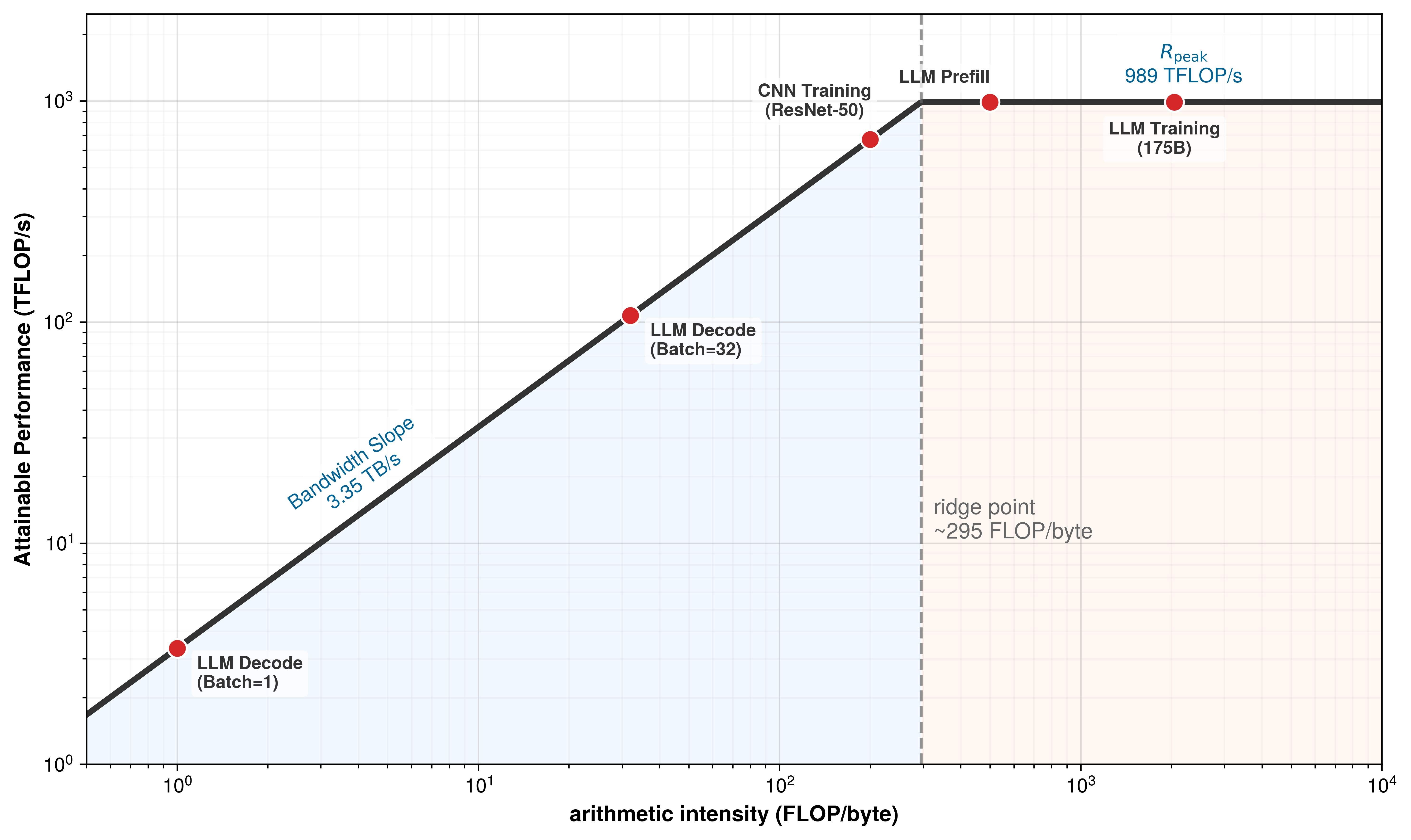
The roofline in figure 9 is defined by two ceilings: memory bandwidth (diagonal) and peak compute (horizontal), meeting at the FP16 ridge point (~295.2 FLOP/byte for 989 TFLOP/s over 3.35 TB/s). ML workloads span the full range: LLM decode at batch size 1 is deeply memory bound, while LLM training at large batch sizes is compute bound. The position of each workload determines whether faster memory or faster compute would improve performance.
The Roofline Model also reveals a subtle but important insight about the interaction between batch size and hardware utilization. Increasing the batch size for a given model raises the arithmetic intensity because the weight matrix is loaded once but multiplied against a larger activation matrix (more FLOPs for the same bytes transferred). This shifts the workload point rightward on the plot, potentially crossing the ridge point from memory-bound to compute-bound territory. The arithmetic intensity grows linearly with batch size (doubling the batch size doubles the FLOPs while keeping the weight loading unchanged), creating a simple and predictable relationship between batch size and hardware utilization.
For inference serving, batching multiple requests together dramatically increases hardware utilization and throughput. A model that achieves 1 percent of peak FLOP/s at batch size 1 might achieve 50 percent of peak FLOP/s at batch size 64, simply because the weight data loaded from HBM is reused across 64 independent requests rather than one. This 50\(\times\) improvement in hardware utilization comes at a cost: the 64 requests must wait until a full batch is assembled before processing begins, introducing queuing latency. Serving systems must carefully balance this trade-off between throughput (larger batches, higher utilization) and latency (smaller batches, faster response per request).
For training, the batch size is a hyperparameter that affects both statistical convergence and hardware efficiency, creating a trade-off that practitioners must navigate carefully. Larger batch sizes improve hardware utilization (pushing the workload into the compute-bound regime) but may require learning rate adjustments and warmup schedules to maintain training quality. The optimal batch size depends on both the model architecture and the hardware’s Roofline characteristics, creating a cross-disciplinary optimization problem that spans ML theory and systems engineering.
The practical value of the Roofline Model is that it tells us which resource to optimize. If a workload is memory-bound, buying a faster accelerator (more TFLOP/s) yields no benefit; only higher memory bandwidth will help. Conversely, if a workload is compute bound, upgrading HBM generations is wasted money. This diagnostic power is the reason that experienced infrastructure engineers always begin a hardware selection process by computing the arithmetic intensity of their target workload and plotting it against the candidate hardware’s Roofline: the plot immediately reveals which hardware characteristic matters and which is irrelevant.
For our 175B model, training with large batch sizes is compute bound (optimize for TFLOP/s), while serving individual requests is memory bound (optimize for bandwidth). This duality explains why some organizations use different hardware generations for training and inference. An A100, with its lower cost and adequate memory bandwidth, may be more cost-effective for inference than an H100, despite the H100’s higher peak FLOP/s.
The Roofline Model also provides a quantitative framework for evaluating the return on investment of different optimizations. If a workload is 10\(\times\) below the compute ceiling but already touching the bandwidth ceiling, spending engineering effort on kernel optimization (moving toward the compute ceiling) yields no benefit. The effort should instead be directed toward reducing memory traffic (shifting the workload rightward on the plot) through techniques like batching, kernel fusion, or quantization.
The Roofline’s diagnostic power makes it one of the most practically useful analytical tools in the infrastructure engineer’s toolkit. Before committing to any hardware purchase or optimization effort, plotting the workload on the Roofline reveals immediately whether the investment will produce returns. Teams that skip this analysis risk spending months optimizing the wrong resource, an expensive mistake when GPU-hours cost thousands of dollars per day.
The same arithmetic-intensity calculation separates the running model’s inference and training regimes.
Example 1.2: Roofline analysis: Training vs. inference
Consider our 175B model on an H100 with 989 TFLOP/s peak compute and 3.35 TB/s memory bandwidth. The ridge point is 295.2 FLOP/byte.
Inference (decode, batch size 1): Each token loads 350 GB of FP16 weights and performs \(2 \times 175 \times 10^9\) FLOPs. Arithmetic intensity: \(I =\) \(\frac{2 \times 175 \times 10^9}{350 \times 10^9} = 1\) FLOP/byte. Since 1 FLOP/byte \(\ll\) 295.2 FLOP/byte (the ridge point), the workload is deeply memory bound. The achievable throughput is \(3.35 \times 1 = 3.35\) TFLOP/s, which is about 0.34 percent of the H100’s peak 989 TFLOP/s. No amount of additional compute will help; only more memory bandwidth improves throughput.
Training forward pass (batch size 2048): The same weight tensor is multiplied by a batch of 2048 activation vectors simultaneously, turning matrix-vector operations into matrix-matrix operations. The FLOPs increase by 2048\(\times\) while the weight loading remains constant: \(I =\) \(2048 \times 1 = 2,048\) FLOP/byte. Since 2,048 FLOP/byte \(\gg\) 295.2 FLOP/byte, the workload is compute bound. The achievable throughput is now limited by the peak compute ceiling of 989 TFLOP/s, and the memory bandwidth is irrelevant. Adding more TFLOP/s (through a newer GPU generation) directly improves performance.
Systems insight: The contrast explains why organizations sometimes use different hardware for training and inference: training benefits from peak FLOP/s, while inference benefits from memory bandwidth per dollar.
That same diagnostic becomes most valuable when a proposed upgrade changes the wrong ceiling.
Checkpoint 1.2: Roofline diagnosis
A team is serving a 13B-parameter model at batch size 1 on an H100 and observing 25 ms per token. The profile shows low tensor-core utilization during decode.
Tensor Cores and matrix units
The Roofline Model tells us whether a workload can reach peak compute. The next question is what determines that peak in the first place. The answer lies in the specialized arithmetic units that occupy the majority of a modern accelerator’s die area: Tensor Cores8 on NVIDIA GPUs and Matrix Multiply Units (MXUs) on Google TPUs.
8 Tensor Core: Introduced with NVIDIA Volta (2017) as \(4{\times}4{\times}4\) FP16 fused matrix-multiply-accumulate units. Each generation widened the tile: Turing (2018) added INT8, Ampere (2020) added TF32/BF16, and Hopper (2022) reached \(16{\times}16{\times}16\) with FP8 support. This precision cascade tracks ML’s own shift toward lower-precision training and inference—each new format unlocks a \(2\times\) throughput gain on the same silicon, making Tensor Core generations a proxy for how quickly the hardware-software co-design loop can widen the Roofline’s compute ceiling.
A standard CPU floating-point unit performs one multiply-accumulate per cycle per lane. Even with wide SIMD units (AVX-512 provides 16 FP32 lanes), a CPU core performs at most 16 MACs per cycle. With 32 cores, a high-end server CPU achieves approximately 512 MACs per cycle, a respectable number for general-purpose computation but wholly inadequate for the demands of matrix multiplication at neural network scale.
A Tensor Core, by contrast, executes matrix-multiply-accumulate (MMA) instructions of the form \(\mathbf{Y} = \mathbf{A} \times \mathbf{B} + \mathbf{C}\) on small tile matrices in specialized hardware. On the H100, these tile operations are distributed across the Tensor Core array in each SM, producing hundreds of accumulated results per instruction while keeping operands in registers and shared memory. This concentrates the dominant neural-network operation in hardware that occupies a small fraction of the chip area.
With 528 Tensor Cores across the chip (4 per SM, 132 SMs), the H100 reaches the 989 TFLOP/s FP16/BF16 peak used in the roofline analysis. The important systems point is not the exact per-cycle instruction accounting, but the architectural specialization: the die dedicates a large fraction of its arithmetic area to dense tiled matrix operations rather than general-purpose scalar execution.
Google’s MXUs take the same concept further by organizing the multipliers into a systolic array. In a systolic MXU, one matrix is loaded into the array’s weight registers while the other matrix streams through the array one row at a time. Each cell multiplies the incoming activation by its stored weight, adds the result to the partial sum flowing from the cell above, and passes both the activation rightward and the partial sum downward. This pipelined flow means the array is performing useful computation on every cycle, with no idle cells once the pipeline is full. The TPU v5p contains two \(128{\times}128\) MXUs per chip, providing 459 TFLOP/s of BF16 throughput. The systolic dataflow eliminates the register file accesses between operations that a Tensor Core still requires, achieving marginally higher energy efficiency at the cost of the flexibility to run nonmatrix workloads.
For our 175B model, the choice between Tensor Cores and MXUs manifests in the compiler stack. CUDA kernels can intermix Tensor Core operations with arbitrary thread-level code, enabling fused kernels that combine matrix multiplies with activation functions, dropout, and layer normalization in a single launch. This fusion is critical for performance because it eliminates the intermediate memory reads and writes that would otherwise occur between operations, keeping data in registers and shared memory where access is fastest.
XLA compilation for TPUs must decompose the computation into sequences of matrix operations that map onto the systolic dataflow, which can be more efficient for standard Transformer architectures but less flexible for custom operations. The XLA compiler performs whole-program optimization, analyzing the entire computation graph to find the optimal tiling, memory layout, and execution schedule for the systolic array. For standard Transformer layers, this whole-program optimization can achieve higher hardware utilization than hand-tuned CUDA kernels, because the compiler can reason about the entire computation rather than optimizing individual operations in isolation.
The hardware dictates the software abstraction, which in turn shapes what architectures are practical to experiment with. This coupling between hardware and software is a defining characteristic of ML infrastructure and explains why hardware selection has downstream effects on research velocity and model design flexibility.
Definition 1.3: Tensor core
Tensor Core is a specialized ML accelerator hardware unit that performs a fused matrix-multiply-accumulate (MMA) operation \(\mathbf{Y} = \mathbf{A} \times \mathbf{B} + \mathbf{C}\) on small tiles (for example, \(16{\times}8{\times}16\) in BF16) as a single hardware instruction, delivering dramatically higher throughput than general-purpose CUDA cores by trading programmability for fixed-function matrix arithmetic.
- Significance: Tensor Cores provide the bulk of the H100’s 989 TFLOP/s FP16/BF16 peak (and ~1,979 TFLOP/s at FP8)—roughly 14.8× the ~67 TFLOP/s delivered by CUDA (vector) cores alone. However, this peak is only achievable for operations that decompose into tiled matrix multiplications. Layer normalization and softmax, which involve reductions and element-wise operations rather than matrix multiplications, run at approximately 3–8 percent of peak throughput on the same hardware.
- Distinction: Unlike general-purpose CUDA cores (which execute one floating-point operation per clock per lane in a SIMT pipeline), Tensor Cores execute 512 multiply-accumulate operations per clock per warp on matrix tiles—trading the arbitrary per-element programmability of CUDA cores for the specific throughput of matrix arithmetic.
- Common pitfall: A frequent misconception is that all GPU operations benefit from Tensor Cores. Only operations that map to the \(\mathbf{Y} = \mathbf{A} \times \mathbf{B} + \mathbf{C}\) tile computation (dense linear layers, attention score computation, convolutions) engage Tensor Cores; element-wise activations, layer norm, and embedding lookups fall back to CUDA cores and can run 10–30\(\times\) slower per FLOP than Tensor Core operations.
The precision support of Tensor Cores has expanded with each generation, driven by the discovery that neural network training and inference can tolerate lower numerical precision than was previously assumed. The Volta generation supported only FP16 accumulation. Ampere added BF16, TF32, and INT8. Hopper added FP8 (both E4M3 and E5M2 formats) with dynamic per-tensor scaling through the Transformer Engine.
The Transformer Engine automatically monitors the magnitude distribution of each tensor and selects FP8 when precision is adequate or FP16 when higher precision is needed, doubling the effective throughput for layers where FP8 suffices. This hardware-assisted precision management represents a convergence of arithmetic design and model-level insight: the hardware is no longer a passive executor of the programmer’s precision choices but an active participant in the precision decision.
Understanding the distinction between the two FP8 formats clarifies why this matters for practitioners. The E4M3 format (4 exponent bits, 3 mantissa bits) can represent values up to approximately \(4.48 \times 10^{2}\), with 3 bits of mantissa providing about 1 part in 8 relative precision. This range and precision are adequate for many neural network weights and activations after per-tensor scaling brings their observed range into the FP8 window.
The E5M2 format (5 exponent bits, 2 mantissa bits) provides a wider dynamic range, with maximum finite values around \(5.73 \times 10^{4}\), at the cost of reduced precision (only 2 mantissa bits, or about 1 part in 4 relative precision). This wider range is important for gradients during the backward pass, which can span more orders of magnitude than forward-pass activations, particularly in the early and late layers of deep networks.
The Transformer Engine selects between these formats on a per-layer basis, and the per-tensor scaling factors are maintained in a small metadata buffer that adds negligible memory overhead. The scaling factors are updated every few iterations based on the observed tensor value distributions, ensuring that the limited precision of FP8 is focused on the range of values that actually appear in each tensor.
The practical implication for fleet design is that peak TFLOP/s specifications are precision-dependent. The H100 delivers 989 TFLOP/s in FP16 but twice that (1,979 TFLOP/s) in FP8. A fleet designed for FP8 training effectively has twice the compute density of the same fleet running FP16, with no additional hardware. This makes precision engineering a first-class optimization lever for infrastructure planners, not just a model accuracy concern.
To achieve this peak throughput in practice, the entire accelerator must be viewed as a rigid pipeline where data flows from HBM through a deepening hierarchy of caches before reaching the Tensor Cores. The fundamental constraint is pipeline balance: the rate at which data is staged into registers must match or exceed the rate at which the arithmetic units consume it. When the arithmetic intensity of an operation falls below the ridge point, the pipeline stalls, leaving teraflops of compute potential idle while waiting for data. This makes kernel fusion the single most critical software optimization for large-scale training. By fusing multiple operations (matrix multiplication, bias addition, activation function) into a single kernel, the system eliminates the round-trips to HBM that would occur if each operation were executed sequentially. Consider the attention mechanism: a naive, unfused implementation writes the \(S{\times}S\) attention matrix to HBM only to read it back for the softmax operation, creating a round trip capped by the 3.35 TB/s memory bandwidth. A fused implementation like FlashAttention keeps these intermediate matrices entirely in on-chip SRAM, bypassing HBM and allowing the Tensor Cores to run near their theoretical peak. For our 175B model, where each training step involves thousands of matrix operations across 96 Transformer layers, the difference between fused and unfused kernels can be a 2–3\(\times\) throughput improvement, separating a 2-week training run from a 6-week one.
Peak vs. sustained throughput
A critical distinction for infrastructure planning is the difference between peak throughput (the maximum the hardware can achieve on a synthetic benchmark) and sustained throughput (what the hardware actually delivers during real training runs). Peak TFLOP/s assumes that the Tensor Cores are fed with data on every cycle, which requires perfect scheduling, zero memory stalls, and no communication overhead. In practice, sustained throughput during Transformer training is typically 30–50 percent of peak for compute-bound operations and less than 5 percent of peak for memory-bound operations. The gap between peak and sustained throughput arises from several sources, each of which represents a different physical or software limitation.
Memory stalls occur when the Tensor Cores complete their current tile multiplication before the next tile has been loaded from HBM. Even with the H100’s 3.35 TB/s HBM bandwidth, the Tensor Cores can consume data faster than HBM can deliver it for certain matrix dimensions, creating idle cycles while the arithmetic units wait for data.
Pipeline bubbles arise when one operation must complete before the next can begin, leaving some processing elements idle. In a Transformer layer, the attention computation must complete before the feed-forward network can begin, and the feed-forward computation must complete before the next layer’s attention can start. These sequential dependencies create brief periods where some hardware resources are unused. The local mechanism is simple: a bubble is an idle slot between dependent stages, and microbatching reduces the waste by feeding later microbatches into stages that would otherwise wait. At the infrastructure level, the lesson is that peak throughput assumes a perfectly filled pipeline, while real training includes dependency gaps that lower sustained utilization.
Communication overhead from AllReduce operations (for tensor parallelism) or gradient synchronization (for data parallelism) pauses computation entirely while data is exchanged between accelerators. Even when communication is overlapped with computation (using separate communication and compute streams), there are typically operations that cannot be overlapped because they depend on the result of the communication.
Software overhead from kernel launch latency, memory allocation, and Python-level control flow contributes an additional 5–10 percent overhead. Each CUDA kernel launch incurs approximately 5–10 microseconds of latency on the host side, and a single Transformer layer may involve 20–30 kernel launches. For small microbatches where each kernel completes in microseconds, the launch overhead can become a meaningful fraction of total execution time.
Kernel fusion partially addresses this gap by combining multiple operations (matrix multiply, bias add, activation function, dropout) into a single GPU kernel, eliminating the intermediate memory reads and writes that would otherwise stall the Tensor Cores between operations. The art of achieving high sustained utilization is largely the art of minimizing the time Tensor Cores spend idle, which is why specialized kernel libraries like FlashAttention and the Transformer Engine exist.
For capacity planning, the sustained throughput rate, not the peak rate, should be used. A training run estimated at 1,000 GPU-hours using peak FLOP/s will actually require 2,000–3,000 GPU-hours when accounting for real-world utilization. Experienced infrastructure teams track their Model FLOPs Utilization (MFU), defined as the ratio of the model’s useful FLOP count to the product of hardware peak FLOP/s and wall-clock time, as the primary metric for infrastructure efficiency. MFU values of 40–50 percent are considered good for large-scale transformer training; values above 50 percent indicate excellent software optimization. The fleet efficiency metric formalizes MFU and develops its fleet-scale application.
Power wall and thermal constraints
The memory wall constrains how fast data reaches the compute units; the Roofline Model diagnoses whether compute or memory is the binding constraint; and Tensor Cores maximize the arithmetic value of every byte fetched. A third physical constraint also limits the accelerator’s performance: the heat generated by all this computation. Every FLOP dissipates energy, and the faster we compute, the more heat we must remove. This is the power wall. Figure 10 traces the journey of energy from grid to transistor.

The cascade shown in figure 10 reveals why power delivery is an infrastructure problem, not merely an electrical one: these conversion losses, combined with the overhead of removing heat, determine the facility’s total power draw, and the 10–40 kW concentrated at the rack PDU-to-VRM transition dictates the cooling architecture for the entire facility. Equation 2 captures that cooling overhead through a single facility ratio, Power Usage Effectiveness (PUE):
\[ \text{PUE} = \frac{P_{\text{facility}}}{P_{\text{IT}}} \tag{2}\]
Here \(P_{\text{facility}}\) is total power drawn by the data center and \(P_{\text{IT}}\) is the power consumed by servers, accelerators, storage, and networking equipment. A PUE of 1.5 means the facility draws 1.5 watts from the grid for every 1 watt delivered to IT equipment; the extra 0.5 watts powers cooling, power conversion, lighting, and other overhead.
Every floating-point operation dissipates energy as heat. Dense Tensor Core activity during large matrix multiplications drives heat proportional to the switching activity of billions of transistors. The Thermal Design Power (TDP)9 of an accelerator is the maximum sustained heat dissipation that the cooling system must handle, and it has become the single most consequential specification in fleet design. At dense fleet scale, this creates the power wall: the point where facility power delivery and heat removal, not available arithmetic units, determine how much compute can be installed and sustained.
9 TDP (Thermal Design Power): Often misunderstood as “power consumption,” TDP specifies the maximum sustained thermal load (in watts) that the cooling solution must remove. Accelerators can briefly exceed their sustained power target during transient workloads before firmware throttles back toward the configured limit, which forces rack-level VRM and cooling designs to provision for worst-case, not average, power draw.
This is the thermodynamic limit (principle 1) in action: the bottleneck of the modern AI data center is not FLOP/s, but Watts per square foot. When a rack generates 100 kW of heat, air cooling fails. The physical design of the fleet is dictated by the ability to move heat away from silicon. The closely related power density wall (principle 2) makes the consequence concrete: liquid cooling becomes a facility requirement, not an option, for large-scale training clusters.
Definition 1.4: Thermal design power (TDP)
Thermal Design Power (TDP) is the maximum sustained thermal load in watts that an ML accelerator’s cooling system must continuously remove for the processor to operate at its rated clock frequency—defining both the cooling infrastructure requirement and the performance ceiling for the accelerator.
- Significance: The H100 SXM5 operates at 700 W TDP. When a liquid cooling system can only sustain 500 W of heat removal (inadequate cooling), the GPU firmware reduces clock frequency via thermal throttling, dropping \(R_{\text{peak}}\) from 989 TFLOP/s to roughly 712 TFLOP/s FP16, a 28 percent reduction in training throughput that propagates directly into longer wall-clock training time and higher cost per model.
- Distinction: Unlike peak power consumption (the instantaneous maximum during a single-instruction burst), TDP specifies the steady-state thermal budget: the long-term average that determines whether training can run continuously at rated performance or must throttle.
- Common pitfall: A frequent misconception is that TDP is a power limit for the software. TDP is a cooling requirement: the processor exceeds its rated speed only if the cooling system removes heat at least as fast as the chip generates it; insufficient cooling causes hardware throttling silently—no error is raised, training simply slows down and MFU drops without obvious cause.
The trajectory of TDP tells the story of a scaling regime reaching its limits. For three decades, Dennard scaling10 allowed chip designers to shrink transistors while maintaining approximately constant power density: smaller transistors required lower voltage, so packing more transistors into the same area did not increase heat output per unit area. As voltage scaling and leakage limits ended that regime, architects had to treat energy, cooling, and parallelism as first-order constraints rather than free byproducts of process shrinks (Dennard et al. 1974; Hennessy and Patterson 2019). Since then, each generation of accelerator has had to trade performance against power and heat. The era of “free” performance improvements through process shrinks is over; every gain in throughput now has to be paid for in watts, cooling capacity, or specialization.
10 Dennard Scaling: Named after Dennard et al. (1974) at IBM, who showed how MOSFET dimensions, voltage, and current could scale so that power density stayed roughly constant. Later voltage-scaling limits and leakage effects ended that constant-power-density regime; Hennessy and Patterson describe the resulting post-Dennard power wall as one reason modern architecture turned toward parallelism and specialization (Hennessy and Patterson 2019). For ML infrastructure, the V100-to-B200 TDP trajectory (300 W to 1,000 W) is an illustration of the post-Dennard planning problem: cooling and power delivery are now co-equal design constraints with the silicon itself.
Dennard, Robert H., Frank H. Gaensslen, Hwa-Nien Yu, Victor L. Rideout, Elias Bassous, and Antoine R. LeBlanc. 1974. “Design of Ion-Implanted MOSFET’s with Very Small Physical Dimensions.” IEEE J. Solid-State Circuits 9 (5): 256–68. https://doi.org/10.1109/jssc.1974.1050511.
Hennessy, John L., and David A. Patterson. 2019. “A New Golden Age for Computer Architecture.” Communications of the ACM 62 (2): 48–60. https://doi.org/10.1145/3282307.
The numbers are stark: the V100 (2017) operated at 300 W TDP, the A100 (2020) increased to 400 W, the H100 (2022) reached 700 W, and the B200 (2024) draws 1000 W. In seven years, TDP has more than tripled, growing at approximately 18 percent per year.
If this growth rate continued as a planning scenario, a generation after Blackwell would approach 1,200–1,400 W per accelerator, and another step could reach 1,500–2,000 W. At 2,000 W per accelerator, a single 8-GPU node would consume 16 kW of GPU power alone, requiring liquid cooling11 infrastructure that can remove heat at rates approaching those of industrial process cooling equipment.
11 Liquid Cooling Flow Rate: A rack of GB200 NVL72 nodes (120 kW) requires approximately 150–200 liters per minute (LPM) of coolant flow. At these rates, the primary risk shift is from thermal throttling to mechanical failure (leaks, pump cavitation), necessitating the industrial-grade manifolds and quick-disconnect fittings common in chemical processing plants.
Systems Perspective 1.2: The end of Dennard scaling
For three decades, Dennard scaling allowed architects to increase transistor count without increasing power density, as smaller transistors required proportionally less voltage. That free lunch ended around 2006 when process nodes dropped below 28nm, where quantum effects like subthreshold leakage and gate oxide tunneling prevent further voltage reduction. The result is that power density rises with transistor density when voltage no longer scales proportionally: accelerators that deliver more TFLOP/s often demand more watts. The transition from the V100 (12nm) to the H100 (4nm) illustrates this physics: while transistor density tripled, the inability to scale voltage meant TDP grew from 300 W to 700 W. The “free” efficiency gains of the silicon era are over; higher performance per watt increasingly comes from architectural specialization – Tensor Cores, systolic arrays, precision engineering – or from accepting higher power and cooling requirements. For ML infrastructure planners, power and cooling capacity must be sized against compute demand, and facility designs cannot assume that later hardware automatically lowers power density.
TDP is not merely a specification on a data sheet; it is a physical constraint that propagates through every level of the infrastructure stack. The power delivery chain, cooling system, rack design, and facility electrical infrastructure must all be designed to accommodate deployed accelerators and the plausible TDP range of future refresh cycles.
Accelerators implement sophisticated power management to operate within their TDP envelope. When the workload does not fully use all SMs (for example, during the communication phase of a training step when the GPUs are waiting for AllReduce to complete), the GPU firmware can disable the clock signal to idle circuitry through clock gating, eliminating dynamic switching power and freeing thermal headroom for the active SMs. A separate mechanism, dynamic voltage and frequency scaling (DVFS), adjusts the chip’s clock frequency and supply voltage to stay within power and thermal limits; during a large matrix multiplication that activates all SMs simultaneously, DVFS reduces the clock frequency to keep total power within TDP. When some SMs are idle, the active SMs can boost frequency because total chip power is below TDP, so the actual clock, and therefore the actual throughput, varies throughout a training step.
Dynamic power management means that the actual power draw of a GPU varies continuously during training. A typical training step might see power swing from 400 W (during communication phases when most SMs are idle) to 700 W (during the forward and backward pass when all Tensor Cores are active) and back, with each transition occurring in microseconds. The VRMs on the baseboard must respond to these transitions fast enough to maintain a stable supply voltage despite the rapidly changing current draw.
To appreciate the physical challenge, consider what 700 W means in terms of heat flux. An H100 die measures approximately 814 mm² (roughly \(29{\times}28\) mm). Dissipating 700 W from this area produces a heat flux of approximately 86 W/cm². For comparison, the surface of an electric stovetop burner at high heat produces approximately 10 W/cm². An H100 die generates 8.6× the heat flux of a stove burner, concentrated on an area the size of a large postage stamp.
The B200 pushes even further: at 1,000 W across a dual-die package, the average heat flux remains comparable, but the total energy that must be removed per package increases by 43 percent. Removing this heat without allowing the junction temperature to exceed 83 degrees Celsius (the typical operating maximum for HBM reliability) requires thermal solutions with extremely low thermal resistance from die to coolant.
The critical component in this thermal path is the Thermal Interface Material (TIM) – the microscopic layer of phase-change material or liquid metal between the silicon die and the cold plate (for liquid cooling) or heatsink (for air cooling). Under the extreme thermal cycling of deep learning workloads, where die temperatures spike from 40 degrees C to 80 degrees C in milliseconds during matrix multiplications and drop back during communication phases, inferior TIM can pump out (migrate away from the contact surface) or crack. A mere 5 percent degradation in TIM thermal conductivity forces the GPU to thermally throttle, reducing clock frequency by hundreds of MHz to protect the silicon. This degradation is a gray failure, a fault that degrades rather than halts: the GPU continues to function, but at reduced performance that silently degrades the entire cluster’s throughput, a failure class we return to in fleet monitoring. Fleet management systems that track per-GPU junction temperatures over time can detect TIM degradation as a gradual upward trend in temperature at constant workload, enabling proactive replacement before the performance impact becomes severe.
At rack scale, four nodes of eight such chips require 33.5 kW of facility-relevant power, enough to heat several homes in winter. To put this in more tangible terms, a single ML rack at full power could run about 33 household space heaters simultaneously, concentrated in a volume roughly the size of a large refrigerator.
At pod scale, the power demand reaches megawatts, requiring dedicated electrical substations and industrial cooling plants. A 10,000-GPU cluster consumes 7–10 MW, comparable to the electrical demand of a large factory or a small town of several thousand residents.
The physical volume of a 10,000-GPU pod operating at this power density is surprisingly compact: the compute hardware (excluding networking and storage) fits in approximately 300 racks, occupying a data center floor area of roughly 1,500 square meters (about one third of an American football field). The density is the point: keeping the accelerators physically close minimizes cable lengths, which reduces signal propagation delay and enables higher interconnect bandwidth.
Physical density, however, makes power delivery and cooling exponentially harder, creating the engineering challenges that define the rack and pod levels of the hierarchy. The paradox of modern ML infrastructure is that computational efficiency demands physical proximity, while thermal management demands physical separation. Every rack design is a negotiation between these opposing forces.
This frequency variability creates a subtle interaction with software optimization. A kernel that achieves high SM occupancy (many active warps per SM) draws more power, potentially triggering a frequency reduction that partially offsets the occupancy benefit. Conversely, a kernel with moderate occupancy may run at a higher clock frequency, achieving comparable throughput at lower power. Power-normalized throughput (TFLOP/s per watt) is therefore a more robust comparison metric than raw TFLOP/s, and it explains why the same GPU can show different sustained clock frequencies depending on the workload and the cooling solution.
At fleet scale, DVFS also affects power planning. The data center’s power delivery must be designed for the worst-case power draw (all GPUs at TDP simultaneously), but the average power draw is typically 70–85 percent of TDP because DVFS reduces frequency during communication phases and because not all SMs are fully occupied at all times. Some operators deliberately set lower power caps on their GPUs (for example, capping an H100 at 600 W instead of 700 W), accepting a 10–15 percent reduction in peak performance in exchange for 15 percent lower power consumption and the ability to fit more GPUs within a fixed power budget. Power capping is a form of the compute-efficiency trade-off at the operational level.
The power efficiency trajectory provides a partial counterweight to rising TDP. While absolute power has increased, the advertised low-precision TFLOP/s delivered per watt has improved dramatically: from 0.42 TFLOPs/s/W (V100 FP16) to 2.83 TFLOPs/s/W (H100 FP8) to 4.50 TFLOPs/s/W (B200 FP8). These are not apples-to-apples FP16 numbers; the precision mode is part of the hardware trend. For a fixed compute budget that can use the newer precision modes, each generation requires fewer chips and therefore less total power. Large-model capability targets, however, can grow faster than efficiency improves, so the absolute power demand of training the next larger model may still increase. This is the treadmill of infrastructure: efficiency gains buy time, but scale growth consumes it.
The implications of TDP for fleet design are profound and will recur throughout this chapter. At the node level, TDP determines how many accelerators can share a single chassis (we examine this in section 1.3). At the rack level, TDP dictates the transition from air cooling to liquid cooling (section 1.4). At the pod level, TDP drives the megawatt-scale power delivery systems that connect the fleet to the electrical grid (section 1.5). The accelerator is the engine, but TDP is the exhaust, and every level of infrastructure above the die exists, in part, to manage that exhaust.
Accelerator selection for ML workloads
An accelerator’s compute throughput, memory bandwidth, memory capacity, and power consumption are meaningful only in relation to a specific workload. The same H100 that delivers near-peak utilization during large-batch training may achieve less than 5 percent utilization during single-request inference, because the binding constraint shifts from arithmetic to memory bandwidth. Selecting the right accelerator therefore requires mapping each workload archetype to its position on the Roofline plot and identifying which physical resource dominates its performance.
Start with the 175B running example. During training, large batches push the forward and backward passes above the Roofline ridge point, so the immediate constraint is arithmetic throughput. Peak low-precision TFLOP/s matters, but only after memory capacity is sufficient to hold the sharded model state and after the interconnect can keep tensor and data parallel groups synchronized. H100, B200, and TPU v5p pods are all plausible answers to this training problem; the final choice depends on the software stack as much as the silicon. A PyTorch-first research team values the GPU ecosystem, while a JAX/XLA-centered organization may accept tighter compilation constraints for TPU cost efficiency.
Serving the same language model changes the answer. During autoregressive decode, every generated token streams weights through memory, so the key metric becomes memory bandwidth per dollar rather than peak TFLOP/s. At batch size 1, the H100’s 3.35 TB/s bandwidth determines throughput while much of the arithmetic silicon waits. Batching raises arithmetic intensity by reusing the same weight movement across more requests, which is why serving systems work so hard to batch without violating tail-latency SLOs. The workload did not change names, but the binding term in the iron law changed, and the accelerator choice changes with it.
Recommendation models split the decision again. Embedding table lookup is dominated by random access and memory capacity, because each request retrieves small vectors from TB-scale tables with poor locality. The dense tower that consumes those embeddings is compute bound. A hybrid CPU-GPU design follows from that split: CPU and DRAM capacity handle the sparse lookup path, while GPUs accelerate the dense neural network layers. A single headline TFLOP/s number cannot describe this workload because it has two different bottlenecks inside one request.
Vision and diffusion workloads move back toward arithmetic throughput because convolutions, attention blocks, and denoising networks reuse data heavily. Diffusion inference makes this especially clear: the Stable Diffusion v1.5 profile in MLSysIM uses 50 denoising steps, so the service pays for a sequence of full model evaluations rather than one decode step per token. For these workloads, TFLOP/s per dollar often dominates bandwidth per dollar once model state fits in memory.
Mixture-of-Experts (MoE) adds a routing constraint: the sparsely gated layer activates only part of a much larger parameter set for each token (Shazeer et al. 2017). Mixtral-8x7B (Jiang et al. 2024), for example, has 46.7B total parameters but only 12.9B active parameters per token because the router chooses 2 experts from 8 experts. That compute saving introduces a many-to-many token exchange pattern, the AllToAll collective examined in Collective Communication, and load-balance risk because tokens must be routed to different expert placements. High-bisection fabrics and load-balancing mechanisms such as auxiliary losses, which penalize overloaded experts, or capacity factors, which cap how many tokens each expert accepts, determine whether the theoretical saving appears in the training trace (Fedus et al. 2022; Lepikhin et al. 2021).
Shazeer, Noam, Azalia Mirhoseini, Krzysztof Maziarz, Andy Davis, Quoc Le, Geoffrey Hinton, and Jeff Dean. 2017. “Outrageously Large Neural Networks: The Sparsely-Gated Mixture-of-Experts Layer.” International Conference on Learning Representations.
Jiang, A. Q., A. Sablayrolles, A. Roux, A. Mensch, B. Savary, C. Bamford, D. S. Chaplot, et al. 2024. “Mixtral of Experts.” arXiv Preprint arXiv:2401.04088.
Fedus, William, Barret Zoph, and Noam Shazeer. 2022. “Switch Transformers: Scaling to Trillion Parameter Models with Simple and Efficient Sparsity.” Journal of Machine Learning Research 23 (120): 1–39.
Lepikhin, Dmitry, HyoukJoong Lee, Yuanzhong Xu, Dehao Chen, Orhan Firat, Yanping Huang, Maxim Krikun, Noam Shazeer, and Zhifeng Chen. 2021. “GShard: Scaling Giant Models with Conditional Computation and Automatic Sharding.” International Conference on Learning Representations.
Multi-modal models add heterogeneity rather than only routing. They combine text decode, vision processing, audio features, and sometimes video, each with different arithmetic intensity and batching behavior. These workloads favor platforms with flexible scheduling and strong bisection bandwidth rather than accelerators optimized for one regular dataflow.
Systems Perspective 1.3: Matching hardware to workload
The fundamental insight from the Roofline Model is that no single accelerator is optimal for all workloads. An H100 that delivers outstanding training throughput for a 175B LLM can sit mostly idle when serving that same model at batch size 1. A TPU pod that provides exceptional cost efficiency for Transformer training may be poorly suited for a recommendation model with irregular memory access patterns.
A mature fleet is therefore heterogeneous by design because each workload makes a different resource decisive. Training clusters spend on arithmetic throughput and fast accelerator-to-accelerator links because synchronization sits in the critical path. Serving clusters spend on memory bandwidth per dollar and latency control because decode streams weights under tail-latency SLOs. Embedding systems spend on DRAM capacity and locality management because sparse lookups dominate the request. Fine-tuning clusters sit between those regimes, balancing memory headroom with enough compute to keep iteration fast. The accelerator spectrum is a design space that must be navigated for each workload independently. Organizations that deploy a single hardware configuration for all workloads inevitably overpay: either the hardware is overprovisioned for simple workloads or underprovisioned for demanding workloads.
Precision and throughput trade-offs
The relationship between numerical precision and hardware throughput is one of the most important considerations for infrastructure planning, because it directly affects how much useful work each accelerator can perform per second. Lower precision representations use fewer bits per number, which has two compounding benefits: more numbers fit in the same HBM capacity (reducing memory pressure), and the arithmetic units can process more operations per cycle (increasing throughput).
The precision landscape for ML has evolved rapidly. Table 6 summarizes representative precision formats on H100-class accelerators and their common use cases.
| Format | Bits | Exponent | Mantissa | H100 Dense TFLOP/s | Typical Use |
|---|---|---|---|---|---|
| FP32 | 32 | 8 | 23 | ~67 | Master weights, loss computation |
| TF32 | 19 | 8 | 10 | 494 | Training (NVIDIA default) |
| BF16 | 16 | 8 | 7 | 989 TFLOP/s | Training, fine-tuning |
| FP16 | 16 | 5 | 10 | 989 TFLOP/s | Training with loss scaling |
| FP8 (E4M3) | 8 | 4 | 3 | 1,979 TFLOP/s | Forward pass, weights |
| FP8 (E5M2) | 8 | 5 | 2 | 1,979 TFLOP/s | Backward pass, gradients |
| INT8 | 8 | N/A | N/A | 1,979 TFLOP/s | Post-training quantization |
| INT4 | 4 | N/A | N/A | 3,958 | Weight-only quantization |
The infrastructure implications are substantial. A fleet designed for BF16 training, a common baseline for large models, delivers 989 TFLOP/s per GPU on an H100. The same fleet running FP8 training delivers 1,979 TFLOP/s per GPU, effectively doubling the compute density without additional hardware. For a 10,000-GPU cluster priced at roughly $350,000 per 8-GPU node, the difference between BF16 and FP8 training is equivalent to adding another 10,000 GPUs, or roughly $438 million in node hardware.
However, not all workloads can use FP8 without accuracy degradation. The reduced mantissa precision (3 bits in E4M3) means that values must be scaled carefully to avoid overflow (values exceeding the representable range saturate or become nonfinite, depending on format and implementation) or underflow (small values rounded to zero). The Transformer Engine’s dynamic per-tensor scaling addresses this challenge for standard Transformer architectures, but custom model architectures with unusual activation distributions may require manual precision tuning. The infrastructure team must therefore work closely with the model team to determine the lowest precision that maintains acceptable accuracy, as this decision directly affects the effective throughput and therefore the required cluster size.
For inference, quantization is one of the most impactful optimizations for serving economics because it directly alters the hardware topology required for large models. Our 175B model at FP16 requires 350 GB, necessitating a minimum of five 80 GB H100 GPUs simply to load the parameters. At INT8, this drops to 175 GB, fitting on three GPUs. At INT4, it shrinks to 87.5 GB, fitting on two GPUs. For memory-bandwidth-bound inference, reading 4-bit weights instead of 16-bit weights effectively quadruples the available bandwidth for weight loading, proportionally reducing per-token latency. A production team deploying at INT4 rather than FP16 can reduce the memory footprint and bandwidth demand of the inference fleet substantially, subject to the quality loss of the chosen quantization method and workload.
For training, many workloads use mixed-precision training, a strategy that decouples storage precision from arithmetic precision. A “master copy” of weights remains in FP32 for numerical stability, while the computationally intensive forward and backward passes are cast to BF16 or FP16 to exploit the full throughput of Tensor Cores. Gradients are accumulated in FP32 to prevent underflow before the optimizer updates the master weights. The H100’s Transformer Engine extends this paradigm by dynamically selecting between FP8 and FP16 on a per-layer basis, potentially doubling throughput again for layers resilient to reduced precision. The cumulative effect on training velocity can be multiple-fold when the model remains numerically stable at the lower precision.
Energy cost of data movement
The Roofline Model and token latency analysis demonstrate that data movement limits performance. Data movement also dominates energy consumption, with direct implications for fleet economics. A useful normalization is an FP16 operand: reading one 16-bit value from HBM at roughly 4 pJ/bit costs about 64 picojoules (pJ), while one FP16 multiply-accumulate (MAC) costs roughly 1 pJ. The raw operand fetch can therefore cost about 64\(\times\) the arithmetic operation, before tiling and reuse amortize that movement across many MACs.

Data movement dwarfs arithmetic in energy cost.
This operand-level ratio explains why accelerator architects devote so much silicon area to data reuse. A Tensor Core’s tile-based execution model loads a small matrix into local registers and reuses each element hundreds of times (once per element in the opposing matrix), amortizing the HBM access cost across hundreds of 1 pJ compute operations. Without this reuse, the energy budget would be dominated by memory access, and most of the chip’s power would be spent heating wires rather than switching transistors.
At fleet scale, the energy cost of data movement determines the electricity bill. For a 10,000-GPU cluster running at 700 W per GPU, approximately 400–500 W per GPU is consumed by the memory subsystem (HBM reads and writes, on-chip network transfers, register file accesses), and only 150–250 W is consumed by the Tensor Cores performing useful arithmetic. The rest goes to clock distribution, I/O, and leakage. Improving data reuse, through techniques like kernel fusion, FlashAttention, and activation checkpointing, reduces the energy wasted on data movement and increases the fraction of power that performs useful computation.
The energy perspective provides a physical foundation for understanding why different parallelism strategies have different efficiencies. Tensor parallelism requires data movement over NVLink (approximately 5 pJ per bit at the link level, plus the energy of the NVSwitch chips). Data parallelism requires data movement over InfiniBand (approximately 15–20 pJ per bit, including the energy of the HCA and switch). Pipeline parallelism moves less data but requires more complex scheduling. Each parallelism strategy represents a different point in the trade-off between communication energy and computation efficiency.
Napkin Math 1.3: The energy cost of data movement
The iron law of modern computing is that moving data costs significantly more energy than manipulating it. We can prove this by analyzing the energy hierarchy of a single operation at the 4nm process node.
Performing one FP16 multiply-accumulate (MAC) operation – the atomic unit of deep learning – consumes approximately 1 picojoule (pJ). This is the baseline cost of useful work. Reading a single FP16 operand (16 bits) from HBM consumes roughly 4 pJ per bit, totaling 64 pJ. Reading that same operand from off-package DRAM costs approximately 20 pJ per bit, or 320 pJ. The asymmetry is staggering: reading a value from HBM costs 64\(\times\) more energy than computing on it. Retrieving it from standard DRAM costs 320\(\times\) more.
The macro impact appears when serving our 175B model. Generating a single token requires loading the entire 350 GB weight tensor from HBM:
\[\text{Data Movement Energy} = 350 \text{ GB} \times 8 \text{ bits/byte} \times 4 \text{ pJ/bit} \approx \mathbf{11.2 \text{ Joules}}\]
The computational cost for the associated \(\approx\) 175 billion MACs (about 350 billion FLOPs) is trivial by comparison:
\[\text{Computation Energy} = 175 \times 10^9 \text{ MACs} \times 1 \text{ pJ/MAC} \approx \mathbf{0.175 \text{ Joules}}\]
Moving the weights to the compute units consumes 64\(\times\) more energy than the math itself in this simplified decode model. This energy penalty is why HBM is engineered for physical proximity to the GPU die – shorter traces mean less capacitance and lower energy per bit. It also explains why techniques that reduce data movement, such as quantization (moving fewer bits) and kernel fusion (preventing round-trips to memory), are the primary levers for improving both system performance and power efficiency.
Benchmarking accelerator performance
A procurement team comparing accelerators needs a published number that predicts the performance the organization will actually achieve. Peak TFLOP/s, memory bandwidth, and TDP describe potential, not achieved performance, so the decision turns on whose measured results to trust and under what rules they were produced. The industry-standard reference is MLPerf, maintained by MLCommons: MLPerf Training reports the time to train reference models to a target accuracy, and MLPerf Inference reports serving throughput and latency under realistic batching and streaming conditions. Both capture complete system performance, including software stack efficiency, communication overhead, and memory management, not just the raw silicon.
The number that actually predicts an organization’s results is the closed-division result, and understanding why is the core of reading MLPerf well. The closed division requires every submission to use the same model architecture, hyperparameters, and training recipe, isolating the hardware and system software as the only variables and making results directly comparable across vendors. The open division allows arbitrary model modifications, custom kernels, and software optimizations, which demonstrate a platform’s ceiling but make cross-vendor comparison unreliable. Infrastructure teams should weight closed-division results more heavily, because they reflect the performance achievable with standard frameworks and configurations, not the performance achievable only by the vendor’s own optimization team.
For our 175B model, no single benchmark captures the full picture. The training phase is compute bound at large batch sizes, making peak TFLOP/s and scaling efficiency the dominant metrics. The inference phase at batch size 1 is memory-bandwidth-bound, making GB/s per dollar the relevant metric. The fine-tuning phase falls between these extremes, with moderate batch sizes placing the workload near the Roofline ridge point. A comprehensive evaluation must benchmark all three phases on the candidate hardware, using the organization’s actual model and data pipeline rather than relying solely on published MLPerf numbers.
Systems Perspective 1.4: Beyond peak specifications
When evaluating accelerator options, the following metrics provide a more complete picture than peak TFLOP/s alone:
- Model FLOPs utilization (MFU): The ratio of achieved FLOP/s during real training to peak hardware FLOP/s. An MFU of 50 percent means the hardware spends half its time on useful computation and half waiting for data, synchronizing, or idling.
- Time-to-Train (TTT): The wall-clock time to train a reference model to a target metric. This captures all system-level effects that MFU alone does not, including I/O stalls, checkpointing overhead, and job restart delays.
- Cost per Token: For language model training, the total cost (hardware amortization plus electricity) divided by the number of tokens processed. This metric normalizes across different hardware generations, cluster sizes, and pricing models.
- Tokens per Second per Dollar: The inverse of cost per token, useful for comparing the economic efficiency of different systems.
No single metric tells the whole story. A system with high MFU but high cost per GPU-hour may be less economical than a system with lower MFU but cheaper hardware. The right metric depends on whether the organization is optimizing for time (training must finish by a deadline), cost (minimize total expenditure), or throughput (maximize tokens processed per unit time).
Inference-specific infrastructure considerations
While this chapter focuses primarily on training infrastructure (because training drives the most demanding infrastructure requirements), the infrastructure for serving trained models at scale deserves separate attention because the design constraints differ fundamentally from training. Training infrastructure is optimized for throughput: maximizing the total number of tokens processed per unit time across the entire cluster. The workload is a single, long-running job that occupies the full cluster for days or weeks. The communication pattern is predictable and repetitive. The acceptable latency for any individual operation is milliseconds to seconds.
Serving infrastructure is optimized for latency and cost per query: minimizing the time each user waits for a response while keeping the per-query cost low enough for the business model to be viable. The workload consists of millions of independent, short-lived requests arriving at irregular intervals. The communication pattern is minimal (each request is processed independently on a single node or small group of nodes). The acceptable latency is tens of milliseconds for interactive applications.
The differing requirements drive distinct hardware and architecture choices, summarized in table 7.
| Dimension | Training infrastructure | Serving infrastructure |
|---|---|---|
| GPU utilization | Large batch sizes push workloads into the compute-bound regime, so clusters commonly achieve 30–50% MFU. | Low-batch serving is deeply memory bound and can achieve less than 5% MFU, so batching improves utilization at the cost of latency. |
| Model placement | Tensor and pipeline parallelism distribute a single model across many GPUs. | Replicas of the model, or large shards of it, handle independent requests, so memory demand scales with concurrent serving capacity. |
| Network traffic | Gradient synchronization requires high-bandwidth, low-latency inter-GPU communication. | Independent requests need little inter-GPU traffic but substantial client-facing bandwidth for millions of API requests per second. |
| Cost metric | Training cost is a fixed, one-time expenditure measured in dollars per run. | Serving cost is a variable expense measured in dollars per 1,000 tokens generated, and popular models can exceed their training cost within weeks. |
The table shows why serving cannot be planned as training with smaller batches: the optimization target changes from synchronized throughput to latency-bounded, continuously billed requests.
The implication is that effective serving infrastructure often uses different hardware, different software, and different facility designs than the training infrastructure. Some organizations use previous-generation GPUs (A100s) for serving because the memory bandwidth per dollar can be competitive with newer GPUs, and the lower TDP (400 W vs. 700 W) allows higher rack density and lower cooling costs.
The inference workload itself bifurcates into two distinct phases with opposing bottlenecks. The prefill phase processes the input prompt, performing a large matrix-matrix multiplication that is compute bound and achieves high Tensor Core utilization. The decode phase generates tokens one by one, performing matrix-vector multiplications that are deeply memory-bandwidth-bound. To maximize hardware utilization, high-performance serving systems employ continuous batching, which schedules requests at the iteration level rather than the request level. This allows the engine to inject a new prefill computation for a waiting request into the idle compute slots of an ongoing decode batch, dynamically filling the GPU’s arithmetic pipelines. For our 175B model, serving 10,000 requests per second with a 50 ms time-to-first-token service level agreement (SLA) requires distributing traffic across hundreds of 8-GPU replicas (each holding the full model via tensor parallelism), with a load balancer routing requests to the replica with the lowest queue depth. Unlike training, where 99.9 percent reliability can be acceptable with checkpointing, inference architectures must account for tail latency, where a single slow replica can violate the SLA for the entire request batch.
The accelerator decision matrix
A practical decision framework synthesizes these workload-specific characteristics by mapping each archetype (Three systems archetypes) to the hardware resource that dominates its performance and cost. Table 8 makes the selection rule explicit: choose for the binding constraint, not the largest advertised peak number.
| Workload | Binding Constraint | Key Metric | Recommended Class |
|---|---|---|---|
| LLM Training (>100B) | Compute (high batch size) | Peak TFLOP/s, NVLink BW | H100/B200, TPU v5p |
| LLM Inference (batch=1) | Memory bandwidth | GB/s per dollar | A100, H100 (bandwidth/$) |
| LLM Inference (batched) | Compute + bandwidth | TFLOP/s and GB/s | H100, B200 |
| Vision Model Training | Compute (large spatial dims) | Peak TFLOP/s | H100/B200, GPU preferred |
| Recommendation (embeddings) | Memory capacity | GB per dollar | CPU DRAM + GPU hybrid |
| Fine-tuning (<13B) | Memory capacity | HBM capacity | A100 (cost-effective) |
| Research/Prototyping | Flexibility | Software ecosystem | GPU (CUDA), avoid ASICs |
The binding constraint shifts with the lifecycle phase, as table 8 shows for the 175B running example. During training, large batch sizes push the workload into the compute-bound regime, making peak TFLOP/s the dominant metric. The H100 or B200, with their high Tensor Core throughput and fast NVLink for tensor parallelism, are the natural choices. During inference at low batch sizes, the same model becomes deeply memory bound, and the relevant metric shifts to bandwidth per dollar. An A100 with adequate HBM bandwidth at a lower price point may deliver better cost-per-token than an H100 whose additional TFLOP/s go unused.
The organizational dimension adds a further consideration. Research labs that modify model architectures weekly need the flexibility of the GPU’s CUDA ecosystem, where custom kernels can be written and tested in hours. Production teams running a fixed Transformer architecture at scale for months may benefit from TPUs, where the XLA compiler’s whole-program optimization can achieve higher sustained utilization than hand-tuned CUDA kernels for standard operations. Custom ASICs make economic sense only for organizations with enough scale to amortize the $50–$200 million NRE cost and enough workload stability to justify a 2–3 year design cycle. The accelerator spectrum is ultimately an economic question answered at the intersection of workload physics, organizational scale, and time horizon.
Checkpoint 1.3: Accelerator selection
Your team needs to deploy a 70B-parameter model for both training and inference. Training will use batch size 2048 across 256 GPUs for 3 months. Inference will serve 10,000 requests per second at batch size 1 for 2 years.
With the accelerator’s physics established, we face a concrete problem. Our 175B model requires 350 GB of memory for its weights alone in FP16, and Adam-style training state raises the requirement to multiple terabytes once optimizer moments, gradients, and activations are included. A single H100 provides 80 GB of HBM. No single accelerator can hold this model. We must expand to the next physical level: the node, where figure 11 contrasts the two dominant approaches to wiring multiple accelerators within a single chassis.
Self-Check: Question
HBM delivers roughly 16\(\times\) the bandwidth of DDR5 at roughly one-tenth the energy per bit (2 pJ/bit vs. 20 pJ/bit). Which packaging-level mechanism most directly explains both the bandwidth and the energy advantage simultaneously?
- HBM replaces centimeter-scale PCB traces with micrometer-scale TSVs through stacked dies on a silicon interposer, shortening signal paths roughly 1,000\(\times\) so a much wider bus can run at lower per-bit driving current.
- HBM clocks each pin at approximately 16\(\times\) the frequency of DDR5, so the bandwidth and energy advantages both stem from faster signaling.
- HBM uses a DRAM cell technology with intrinsically higher density and lower leakage, which allows both more bits per second and lower energy per access.
- HBM stores weights in a compressed on-die format, so the bandwidth figure reflects decompressed bytes while the energy figure reflects only the compressed bits that cross the bus.
A vendor proposes a successor to the H100 with 2\(\times\) the peak FP8 TFLOP/s but the same 3.35 TB/s HBM bandwidth, targeted at 70B-parameter LLM serving at batch size 1. Using roofline reasoning with the H100’s ridge point near 295 FLOP/byte and decode arithmetic intensity near 1 FLOP/byte, explain why the per-token latency improvement will be negligible and where the same silicon budget would actually produce speedup.
True or False: Once a 70B model’s weights fit in the serving memory system, either through sharding, quantization, or a higher-capacity accelerator, doubling HBM capacity while leaving bandwidth unchanged will substantially cut per-token latency during batch-1 decode.
A GPU profile shows a kernel operating at 1 FLOP/byte while the H100’s ridge point sits near 295 FLOP/byte. Using the iron law decomposition, which lever would most directly raise this kernel’s achieved throughput?
- Raising the accelerator’s peak FP16 TFLOP/s, because moving the horizontal ceiling up increases the attainable FLOP/s at every arithmetic intensity.
- Balancing the workload at the ridge point by padding with extra memory reads, because workloads at the ridge intersect both ceilings and benefit from compute and bandwidth upgrades equally.
- Doubling HBM bandwidth or fusing neighboring kernels so intermediates stay in on-chip SRAM, because the workload sits on the bandwidth-bound slope where achievable FLOP/s equals bandwidth times arithmetic intensity.
- Moving more work onto host CPU preprocessing, because CPU preprocessing is typically the bottleneck whenever GPU utilization is low.
Order the following data path as operand bytes move from their resting place to a Tensor Core during a tiled matrix multiply on an H100: (1) shared memory / SRAM tile, (2) HBM weight tensor, (3) SM register operands feeding the Tensor Core.
An unfused attention implementation writes the attention matrix to HBM after softmax and re-reads it for the subsequent matrix multiply. FlashAttention-style fusion collapses these stages into one launched kernel. Why does this typically speed up the kernel far more than raising peak FLOP/s would?
- Fusion increases HBM capacity, letting larger portions of the model reside permanently on-chip and therefore skip the HBM round-trip.
- Fusion replaces the Tensor Cores with general-purpose CUDA cores whose branchy code runs softmax faster than the matrix units can.
- Fusion raises the kernel’s arithmetic intensity into the compute-bound regime regardless of sequence length or batch size.
- Fusion keeps softmax outputs resident in SRAM across stages, eliminating the HBM write-and-reread that dominates runtime when the kernel is memory-bound.
The Node
The node is the first scale level where accelerator choice becomes an interconnect problem. Multiple GPUs can now share one chassis, but their useful behavior depends on whether the local fabric behaves like a slow ring, a dense mesh, or a switch-backed crossbar.

Aggregating accelerators solves the capacity problem only if the interconnect between them is fast enough that the group behaves as one machine rather than as several machines passing messages. The 175B model’s weights span at least five accelerators, and the full training state spans an entire 8-H100 node and more, so the parameters of a single layer now live on different chips and must be reassembled on every forward and backward pass. Whether that reassembly is cheap or ruinous depends entirely on the local fabric, which is why the node is the first scale level where the accelerator’s specifications matter less than the wires between accelerators. The training system must combine tensor parallelism with optimizer sharding and memory offload, and each of those strategies places a different demand on the interconnect.
Definition 1.5: Node
Node is the ML training cluster’s physical server chassis that aggregates multiple accelerators (typically 8) through a high-speed intra-node interconnect (NVLink or ICI), creating the fundamental boundary between high-bandwidth local communication and the order-of-magnitude slower inter-node network fabric.
- Significance: The NVLink bandwidth within a DGX H100 node reaches 900 GB/s bidirectional, or 450 GB/s per direction, while inter-node InfiniBand NDR provides 50 GB/s, a 9× per-direction gap that constrains where each parallelism strategy can run. Tensor parallelism, which AllReduces every layer’s output, must stay within the node; pipeline parallelism, which transfers only stage-boundary activations, can span nodes over InfiniBand. The node is also the primary failure domain: a single node failure in a bulk synchronous parallel (BSP) training job, where workers advance in lockstep at step barriers, idles the entire cluster until recovery.
- Distinction: Unlike a single accelerator (which provides fast HBM bandwidth but limited capacity), a node aggregates 8\(\times\) the HBM capacity and 8\(\times\) the compute of a single chip – enough to place large FP16 weight shards (8 \(\times\) 80 GB = 640 GB on DGX H100), but not enough to keep the full Adam training state in HBM.
- Common pitfall: A frequent misconception is that nodes in a distributed training job operate independently. In BSP training, all nodes are synchronously coupled at every step barrier: a performance degradation on one node (from thermal throttling, a faulty NIC, or a slow storage read) stalls the entire cluster and drops overall MFU for the duration of that step.
The node exists because of a gap in the memory hierarchy. HBM provides enough bandwidth to feed the accelerator’s arithmetic units, but not enough capacity to hold the full 175B-parameter running example. Host DRAM provides capacity (512 GB to 2 TB per server) but not enough bandwidth.
The node bridges this gap by aggregating the HBM of multiple accelerators into a shared pool, connected by an interconnect fast enough to allow cooperative computation across all of them. The key engineering insight is that by placing 8 accelerators in a single chassis and connecting them with a high-speed fabric, the node creates a virtual accelerator with 8\(\times\) the memory capacity and 8\(\times\) the compute throughput of any individual chip, while the fast interconnect ensures that this virtual accelerator can operate nearly as efficiently as a single monolithic device.
The economic argument for multi-accelerator nodes is equally compelling. Consider the alternative: building a single accelerator with enough HBM to hold a 175B model (350 GB in FP16). Current packages provide roughly 16–24 GB per HBM stack, so a 350 GB single-accelerator design would require on the order of 15–22 HBM stacks – far beyond the 5-stack H100 or 8-stack B200-class package. The manufacturing cost of such a package would be prohibitive (yield decreases with package and interposer area), and the power delivery to a single chip with enough Tensor Cores to use all that bandwidth would exceed any practical cooling solution. By distributing the computation across 8 accelerators connected by NVLink, the node achieves the aggregate memory capacity and compute throughput of this hypothetical super-chip while remaining within manufacturable and coolable boundaries.
Understanding how the node partitions memory across its components is essential for selecting parallelism strategies. Consider the memory budget for training our 175B model. The model weights in FP16 require 350 GB. The Adam optimizer maintains two additional copies of every parameter (first and second moments) in FP32 precision, adding 175 \(\times 10^9 \times 2 \times 4\) bytes = 1,400 GB. Gradients require another 350 GB. The total is approximately 2.1 TB before activations, far exceeding both a single accelerator’s 80 GB HBM and an 8-H100 node’s 640 GB aggregate HBM.
When using ZeRO or FSDP-style optimization (which shards optimizer states, gradients, and optionally parameters across data-parallel workers), the training system avoids replicating this full 2.1 TB state on every GPU. Tensor parallelism first reduces each GPU’s active weight shard; data-parallel sharding then spreads optimizer state and gradients across many workers; activation checkpointing reduces the activation peak; and offload moves cold optimizer state to host DRAM over PCIe. The node is therefore a high-bandwidth compute and communication unit, not a standalone container for the entire training state.
The node’s internal memory hierarchy, consisting of HBM (fast, small), host DRAM (medium speed, larger), and Non-Volatile Memory Express (NVMe) storage (slow, very large), forms a tiered system that distributed training frameworks exploit aggressively. Distributed Training examines these memory optimization strategies in detail.
Bandwidth hierarchy
The defining characteristic of multi-accelerator systems is not the number of chips but the speed at which they can exchange data. Data movement speed drops by orders of magnitude as it crosses physical boundaries. Each boundary represents a different physical medium, a different connector technology, and a different set of engineering constraints. This physical ordering of data transfer rates, from on-chip SRAM at the fast end to the wide-area network at the slow end, is the bandwidth hierarchy, and understanding it is essential because it dictates where in the hierarchy each type of parallelism can operate efficiently.
The hierarchy reflects the physical cost of distance: shorter signal paths over denser wiring achieve higher throughput at lower energy per bit, so at each boundary the effective bandwidth \((\text{BW})\) drops by roughly an order of magnitude while latency \((L_{\text{lat}})\) rises. That gradient sets a scaling ceiling for distributed training. The common mistake is to treat all cluster communication as equal, but parallelism placement must be hierarchy-aware: putting high-frequency synchronization such as tensor parallelism on a slow tier idles the compute units \((R_{\text{peak}})\) and collapses scaling efficiency \((\eta_{\text{scaling}})\).
The bandwidth hierarchy is best understood as a series of concentric zones around each accelerator. The innermost zone is the HBM on the same package, with terabytes per second of bandwidth and sub-microsecond latency. The next zone encompasses the other accelerators within the same node, reachable over NVLink at hundreds of gigabytes per second with microsecond-scale latency. The outermost zone spans all other nodes in the cluster, connected by InfiniBand at tens of gigabytes per second with latency measured in single-digit microseconds. At each zone boundary, the bandwidth drops by roughly an order of magnitude while the latency increases by roughly an order of magnitude. Table 9 maps those zones to the parallelism strategies they can support.
| Domain | Interconnect | Bandwidth | Latency | Scaling Limit |
|---|---|---|---|---|
| Intra-Package | Silicon Interposer | ~3.3 TB/s | <100 ns | Single Chip |
| Intra-Node | NVLink/ICI | ~900 GB/s | ~1 μs | Node (8–16 Chips) |
| Intra-Node (IO) | PCIe Gen5 x16 | ~64 GB/s | ~2 μs | CPU-GPU, NIC-GPU |
| Inter-Node | InfiniBand NDR | ~50 GB/s | ~5–10 μs | Pod (Thousands) |
The concentric view in figure 12 presents the same hierarchy spatially, so each outward boundary crossing reads as both a bandwidth drop and a latency increase.

As table 9 shows, parallelism strategies must respect these boundaries. A simple synchronization calculation makes the bandwidth gaps concrete.
Napkin Math 1.4: The physics of the staircase
Problem: A 10 GB buffer is synchronized across the fleet. How much does the physical “Layer” of the fleet affect transfer time?
Math: Transfer time is \(T_{\text{transfer}} = D_{\text{vol}} / \text{BW}\).
- HBM (intra-chip): 10 GB / 3,350 GB/s \(\approx\) 3.0 ms.
- NVLink (intra-node): 10 GB / 450 GB/s \(\approx\) 22.2 ms.
- InfiniBand (inter-node): 10 GB / 50 GB/s \(\approx\) 200 ms.
Systems insight: Moving data across the cluster is 9× slower than moving it within a node. This “Bandwidth Staircase” is the primary driver of all parallelization strategies: we use tensor parallelism where bandwidth is abundant (NVLink) and data parallelism where it is scarce (InfiniBand). A model that “fits” in memory but ignores the staircase will spend 90 percent of its time waiting for the network.
Each cliff in the bandwidth staircase exists for a different physical reason, rooted in the signal-propagation regime at its distance scale. The intra-package interconnect achieves terabytes per second because signals travel through lithographically patterned copper traces on a silicon interposer, with path lengths measured in millimeters. At these distances, signal attenuation is negligible, no amplification is needed, and the signaling rate is limited only by the trace geometry and the transceiver design.
NVLink achieves hundreds of gigabytes per second using high-speed SerDes12 transceivers over short copper cables or traces within a chassis, with path lengths of tens of centimeters. At these distances, signal attenuation is measurable but manageable with simple equalization circuits. The SerDes transceivers use PAM-4 (4-level pulse amplitude modulation) signaling at 112 Gb/s per lane, packing 2 bits per symbol to double the data rate relative to NRZ (nonreturn-to-zero) signaling.
12 SerDes (Serializer/Deserializer): From Latin serialis (in a row) and de- (reverse). A circuit pair that converts parallel data to a serial bit stream for transmission and back again. Modern high-speed links use PAM-4 signaling (4-level pulse amplitude modulation, encoding 2 bits per symbol) at very high lane rates, and the transceiver energy becomes a material part of node power. This is why dense interconnects such as NVLink, InfiniBand, and PCIe must be treated as power and cooling loads, not just as bandwidth specifications.
PCIe uses a standardized protocol with flow control overhead, reducing effective bandwidth. While PCIe Gen5 uses the same 32 GT/s signaling rate as NVLink’s individual lanes, the protocol overhead (packet headers, flow control credits, error checking) consumes approximately 20 percent of the raw bandwidth. The standardization that makes PCIe universally compatible also makes it less efficient than proprietary interconnects.
InfiniBand crosses meters of cable between racks, requiring signal amplification, error correction, and switch hops that add both latency and protocol overhead. Active optical cables (AOCs) convert electrical signals to light at the transmitter, propagate through optical fiber, and convert back to electrical signals at the receiver. Each electro-optical conversion adds approximately 2–5 nanoseconds of latency and consumes power for the laser driver and photodetector. Switch hops add another 100–300 nanoseconds each for packet routing and buffering.
As table 9 illustrates, the practical consequence is that parallelism strategies must respect these boundaries. Tensor parallelism (TP), which splits individual matrix multiplications across accelerators and requires an AllReduce operation after every layer, generates communication volume proportional to the model’s hidden dimension hundreds of times per second. At NVLink bandwidth, this synchronization takes roughly 1 ms per layer. At InfiniBand bandwidth, the same synchronization takes 10–20 ms, which would leave the accelerators idle for the majority of each training step.
TP is therefore confined to within a single node, while data parallelism (which synchronizes gradients only once per training step) spans the inter-node network. The bandwidth hierarchy is the physical law that determines the topology of distributed training.
The hierarchy also explains why pipeline parallelism occupies an intermediate position in the bandwidth requirements. In pipeline parallelism, the model is divided into sequential stages, with each stage assigned to a different group of accelerators. The communication between stages consists of activations flowing forward during the forward pass and gradients flowing backward during the backward pass, with a volume proportional to the batch size times the hidden dimension.
For our 175B model with hidden dimension 12,288 and a microbatch of 4 sequences at 2,048, the activation tensor at each stage boundary is approximately \(4 \times 2,048 \times 12,288 \times 2 B\) bytes (FP16) \(\approx\) 201 MB. This is far smaller than the 350 GB gradient AllReduce required by data parallelism, which is why pipeline parallelism places less demanding requirements on the inter-node network.
Activation transfers occur once per microbatch per stage boundary, far less frequently than tensor parallelism’s per-layer AllReduce. Pipeline parallelism can therefore tolerate the lower bandwidth of inter-node links, making it the preferred strategy for spanning multiple nodes when the model’s depth exceeds a single node’s capacity.
The result is a natural mapping between parallelism types and interconnect domains: tensor parallelism within the node (NVLink), pipeline parallelism across nearby nodes (InfiniBand), and data parallelism across the full cluster (InfiniBand with gradient compression). This mapping is so fundamental that it has become a de facto standard in production-scale Transformer training systems, with the details differing primarily in the number of pipeline stages, the degree of tensor parallelism, and the degree of data parallelism.
The mapping also determines how the job scheduler assigns nodes to training jobs. Nodes within the same tensor-parallel group should be physically adjacent (ideally in the same chassis, connected via NVLink). Nodes within the same pipeline-parallel group should be in the same rack or adjacent racks (minimizing InfiniBand switch hops). Data-parallel groups can span the entire cluster because their communication (gradient AllReduce) is the least bandwidth-intensive and most latency-tolerant of the three parallelism types. One intra-node boundary remains before that mapping reaches the scheduler: the PCIe hierarchy that connects accelerators to host CPUs, NICs, storage, and DRAM.
The PCIe hierarchy within a node
While NVLink provides a high-bandwidth freeway for GPU-to-GPU communication, PCIe Gen5 serves as the universal glue connecting the heterogeneous components of the node. It links GPUs to the host CPU, GPUs to InfiniBand Host Channel Adapters (HCAs), the host CPU to NVMe storage, and the host CPU to system DRAM. Understanding this topology is critical because PCIe bandwidth – though substantial at ~64 GB/s per direction (128 GB/s bidirectional) per x16 link – is often the bottleneck for operations that cross the accelerator boundary, such as data loading, checkpointing, and inter-node gradient synchronization.
A standard DGX H100 node features two host CPUs, each managing a PCIe root complex with 128 lanes. These lanes are distributed to maximize simultaneous throughput: 8 GPUs each receive a dedicated x16 link, and 8 InfiniBand HCAs each receive their own x16 link. This configuration provides an aggregate theoretical bandwidth of nearly 2 TB/s within the chassis. However, this bandwidth is shared among competing traffic streams. During a single training step, the PCIe bus simultaneously carries host-to-GPU data batches, GPU-to-HCA gradient shards for inter-node AllReduce (via GPUDirect RDMA), and periodic CPU-to-NVMe checkpoint writes. Contention between these streams can cause unexpected pipeline stalls, particularly when gradient synchronization saturates the links typically used for data loading.
The dual-CPU architecture introduces significant Non-Uniform Memory Access (NUMA) effects. The 8 GPUs are physically partitioned, with 4 connected to CPU 0’s root complex and 4 to CPU 1’s. A GPU connected to CPU 0 can access CPU 0’s DRAM at full PCIe bandwidth but must traverse the inter-processor interconnect (UPI or Infinity Fabric) to access CPU 1’s DRAM. This traversal incurs additional latency and reduces effective bandwidth by up to 50 percent. Robust data loading pipelines must employ NUMA-aware scheduling, pinning data loader worker processes to the CPU cores physically closest to the target GPUs. Empirical benchmarks show that aligning data loaders with the correct NUMA domain can improve data ingestion throughput by 20–30 percent, preventing the CPU from becoming the bottleneck in high-throughput training runs.
The practical consequence is that placement is part of the parallelism strategy: a scheduler that ignores PCIe roots, NIC locality, and NUMA domains can turn an otherwise valid tensor- or pipeline-parallel plan into a host-bound bottleneck. Distributed Training formalizes how these intra-node and inter-node boundaries interact with data, tensor, and pipeline parallelism.
Dense node designs
Given the bandwidth hierarchy, the engineering challenge within a node is clear: connect 8 accelerators with enough bandwidth that they can function as a single logical device for tensor-parallel operations. The solution is a specialized switching fabric that provides full bisection bandwidth between all accelerator pairs. Understanding the design of this fabric requires appreciating why simpler alternatives fail.
The simplest approach would be to connect the 8 GPUs in a ring, where each GPU has links to its two neighbors. A ring is inexpensive (requiring only \(N\) links for \(N\) GPUs) and works well for ring-AllReduce, where data flows sequentially around the ring in a circular pattern. The ring-AllReduce algorithm achieves optimal bandwidth utilization for gradient synchronization because each GPU simultaneously sends data to its right neighbor and receives data from its left neighbor, keeping all links busy throughout the operation.
However, tensor parallelism requires all-to-all communication: every GPU must exchange partial results with every other GPU after each layer. This is a fundamentally different communication pattern from the sequential flow of ring-AllReduce, and the ring topology handles it poorly. In a ring of 8 GPUs, communicating between opposite sides requires 4 hops, reducing effective bandwidth by 4\(\times\) compared to a direct link. A fully connected mesh, where every GPU has a direct link to every other GPU, eliminates this problem but requires \(N(N-1) / 2 = 28\) links for 8 GPUs, a wiring challenge that becomes impractical as the link count grows quadratically. The NVSwitch crossbar provides the best of both worlds: full bisection bandwidth with a manageable number of switch chips.
Consider the NVIDIA DGX H100 architecture. Eight H100 GPUs sit on a single baseboard, each connected to four NVSwitch chips via 18 NVLink 4.0 lanes. The NVSwitch chips form a non-blocking crossbar13: any GPU can communicate with any other GPU at the full 900 GB/s bidirectional bandwidth simultaneously, without contention. This is the equivalent of giving every pair of GPUs their own private highway, rather than forcing them to share a single road.
13 Crossbar Switch: A topology providing a dedicated path between every input-output pair simultaneously. An \(N{\times}N\) crossbar has \(N^2\) crosspoints, achieving full bisection bandwidth. NVSwitch implements a 3-stage crossbar using four switch chips (each with 64 NVLink ports), consuming ~800 W total – more than an entire V100 GPU – but this power cost is justified because it enables all-to-all tensor parallelism within a node, the communication pattern that would otherwise dominate training time.
The result is that the 8 GPUs within a DGX H100 can be treated as a single logical device with 640 GB of aggregate HBM and a combined compute throughput of 8 \(\times\) 1979 TFLOP/s. This abstraction is critical for software: the training framework can partition a model across the 8 GPUs using tensor parallelism as if they were a single larger processor, with the NVSwitch fabric making the partitioning nearly transparent from a performance perspective.
The physical layout of the DGX H100 baseboard reflects this design goal. The 8 GPUs are arranged on the baseboard with the 4 NVSwitch chips positioned centrally. Each GPU connects to all 4 NVSwitch chips via NVLink lanes, and each NVSwitch chip has 64 NVLink ports that cross-connect the GPUs.
The NVSwitch chips themselves consume approximately 200 W each (800 W total for the NVSwitch fabric), a nontrivial power overhead that is justified by the bisection bandwidth it provides. To put this in perspective, the NVSwitch fabric alone consumes more power than an entire previous-generation GPU (the V100 drew 300 W). Without NVSwitch, achieving full all-to-all connectivity would require 28 direct GPU-to-GPU links, a wiring nightmare that would also consume more total NVLink lane capacity.
During a tensor-parallel forward pass, each GPU holds one shard of each weight matrix and computes its portion of the matrix multiplication. For a Transformer layer with hidden dimension 12,288 (typical for a 175B model), each of the 8 GPUs holds a \(12{,}288{\times}1{,}536\) slice of the weight matrix. After each GPU computes its partial result, an AllReduce operation sums the partial results across all 8 GPUs over NVLink.
The AllReduce for a single layer’s output involves exchanging approximately \(4 \times 2{,}048 \times 12{,}288 \times 2\) bytes (FP16) across the NVLink fabric. For a typical microbatch size of 4 sequences at 2,048 tokens, this is roughly 201 MB per AllReduce, which completes in about 0.2 ms at 900 GB/s.
Even with 96 layers (forward pass) and 96 layers (backward pass), the cumulative AllReduce time is about 42.9 ms per training step. This is possible because the NVSwitch crossbar allows all 8 GPUs to communicate simultaneously without contention, unlike a ring topology where data must traverse multiple hops sequentially.
The communication overhead is small relative to the compute time per layer, which is approximately 2–5 ms depending on the sequence length and batch size. The resulting tensor-parallel scaling efficiency within the node is typically 85–95 percent, meaning that using 8 GPUs achieves 6.8–7.6\(\times\) the throughput of a single GPU.
The remaining 5–15 percent efficiency loss comes from two sources. First, the AllReduce communication itself, even at NVLink bandwidth, consumes a fraction of each layer’s execution time. Second, some operations in the Transformer (layer normalization, dropout, activation functions) are not tensor-parallelized because their computation is small relative to the matrix multiplications. These sequential operations must complete on every GPU before the next layer’s tensor-parallel computation can begin, introducing small but cumulative idle time.
Example 1.3: The NVLink bandwidth surprise
Scenario: Early users of multi-GPU nodes often attempted tensor parallelism over PCIe, expecting the 64 GB/s bandwidth to suffice.
Diagnosis: Tensor parallelism requires AllReduce after every Transformer layer, not just once per training step. A model with 96 layers generates 96 AllReduce operations per forward pass and another 96 during the backward pass, totaling 192 synchronization events per step. At PCIe bandwidth, each AllReduce for a 12,288-dimensional hidden state takes approximately 3.1 ms, accumulating to 604 ms of pure communication overhead per step. With a 200 ms compute-step anchor, the accelerators spend roughly 75.1 percent of their time waiting for PCIe transfers. Switching to NVLink reduces each AllReduce to 0.2 ms, bringing total communication overhead to 42.9 ms and restoring accelerator utilization to over 82.3 percent.
Systems lesson: For tensor parallelism, the interconnect is the bottleneck, and the difference between PCIe and NVLink is not incremental; it is the difference between a functional and a nonfunctional system.
Beyond NVLink, the node also connects to the external network via InfiniBand Host Channel Adapters (HCAs) and to host storage via PCIe. The DGX H100 includes eight InfiniBand ConnectX-7 HCAs, one per GPU, enabling GPUDirect RDMA: the network adapter can read from and write to GPU HBM directly, without staging data through host DRAM or involving the host CPU in the data path.
GPUDirect RDMA is critical for inter-node gradient synchronization, where each GPU’s gradient shard must be sent to its peers on other nodes. Without GPUDirect, each gradient transfer would require two extra copies: first from GPU HBM to host DRAM (over PCIe), and then from host DRAM to the network adapter (over another PCIe path). The double-copy adds latency (two PCIe traversals instead of one direct DMA operation) and halves the effective bandwidth (each byte traverses the PCIe bus twice).
GPUDirect RDMA eliminates both copies by allowing the InfiniBand HCA to read directly from GPU HBM, bypassing the host CPU and host DRAM entirely. The data path goes from GPU HBM through the NVLink-to-PCIe bridge to the InfiniBand HCA in a single transfer. The single-hop data path is one of the reasons that modern training clusters achieve inter-node communication bandwidth close to the raw InfiniBand line rate.
The host CPU manages job scheduling, data preprocessing, data loading from storage, and network protocol processing, but it sits outside the critical path of the GPU-to-GPU computation. The separation is deliberate: the host handles the “slow” operations (disk I/O, network management, job coordination) while the GPU-NVSwitch fabric handles the “fast” operations (matrix math, gradient synchronization).
The host CPU’s role is analogous to an operating system kernel in a traditional computer: it manages resources, handles exceptions, and coordinates I/O, but it does not perform the application’s core computation. In a well-optimized training loop, the host CPU is almost never on the critical path, and its performance specifications (core count, clock speed) are less important than its I/O capabilities (PCIe lane count, memory channels, NVMe controller bandwidth).
The host CPU also runs the training framework’s Python runtime, which orchestrates kernel launches, manages the computation graph, and coordinates collective communication operations. In well-optimized training loops, the host CPU is pipelining the next batch’s data loading and preprocessing while the GPUs are executing the current batch’s forward and backward passes, keeping all components busy simultaneously.
As the “data center tax” on host CPUs has grown – with up to 30 percent of CPU cycles consumed by network protocol processing, storage virtualization, and security functions – ML nodes can incorporate Data Processing Units (DPUs) or SmartNICs. Devices like the NVIDIA BlueField DPU offload these infrastructure tasks to dedicated ARM cores and hardware accelerators integrated into the network adapter itself. By moving the control plane for RDMA, firewall rules, and storage protocols to the DPU, the host CPU recovers cycles for the ML pipeline: data loading, tokenization, and kernel orchestration. The DPU also acts as an isolated security domain, allowing cloud providers to maintain control over the network and storage layer via the DPU while granting customers full access to the host CPU and GPUs. For our 175B model training, DPU offload can keep RDMA protocol processing outside the host CPU critical path for gradient synchronization, which flows from GPU HBM toward the network fabric without host CPU involvement.
Alternative node architectures
These alternatives are accelerator-system designs, not interchangeable product names. An AMD MI300X is a GPU-class accelerator whose package emphasizes very large HBM capacity, while Intel/Habana Gaudi designs emphasize Ethernet/RDMA attachment as a first-class communication path. Comparing them against a DGX H100 node reveals where each architecture spends its scarce budget.
The DGX H100 answers a general node-design problem by making local accelerator exchange cheap. A switch-rich design spends power, board area, and cost on universal any-to-any exchange. That choice is easy to justify when tensor parallelism is the critical path, because each Transformer layer turns local accelerator communication into part of the model’s inner loop. The 900 GB/s H100 NVLink fabric therefore buys a software abstraction: the training framework can treat eight accelerators as one tightly coupled device for the layers that must be split across chips.
Other systems move that boundary. TPU pods use the Inter-Chip Interconnect (ICI) and a mesh-oriented topology instead of making a central switch the defining component of the node; the TPU v5p profile in MLSysIM models ICI at 1,200 GB/s. The mesh can reduce switch cost and expose a regular structure to the compiler, but it also makes placement more visible: the runtime must respect neighbor relationships rather than assuming that every chip pair has the same communication path. That is a reasonable trade when the workload is regular enough for the compiler and collective libraries to map communication onto the topology.
The MI300X shifts the pressure point from local switching toward memory capacity. Its package exposes 192 GB of HBM at 5.3 TB/s, compared with 80 GB on an H100-class accelerator. An eight-accelerator MI300X node would therefore provide 1,536 GB of aggregate HBM, enough to hold the 350 GB FP16 weight tensor for our 175B running model. That does not eliminate the optimizer, gradient, activation, and fragmentation problem introduced in section 1.3, but it changes how often the system must spill state into slower memory tiers and how much microbatch headroom remains before offload becomes mandatory.
Gaudi takes a different route by integrating RDMA-capable Ethernet into the accelerator and using a more network-centric design for communication. The Gaudi 2 profile exposes 300 GB/s of aggregate RoCE bandwidth through 24 attached 100 GbE ports, while an H100-class NVLink node offers 900 GB/s of local GPU exchange and the newer Gaudi 3-class accelerator still exposes 128 GB of HBM. The question is whether simplifying the fabric and using Ethernet consistently across node and pod is worth giving up the very high local exchange bandwidth of a switch-rich NVLink design. That trade can be attractive when data parallelism, inference serving, or cluster cost dominates, and less attractive when tensor-parallel collectives sit inside every layer.
These alternatives are not a ranking of vendors. They are different placements of scarce resources: switching bandwidth in the node, regular topology in the pod, HBM capacity in the package, or network attachment on the accelerator. For the 175B model used throughout this chapter, the tensor-parallel portion of training makes local accelerator communication unusually important, so the DGX-style answer is natural. In other regimes, especially memory-heavy recommenders, topology-regular training, or cost-sensitive serving fleets, a different boundary can become the one that matters most. Software ecosystem maturity, supply availability, and total cost of ownership then decide whether the theoretical architectural fit becomes a deployable system.
Node health and reliability
The node is the fundamental failure domain in the fleet hierarchy. When a single GPU fails within a node, the entire node typically becomes unusable for the training job, because tensor parallelism requires all 8 GPUs to participate in every AllReduce operation. A single missing GPU breaks the collective communication, stalling all other GPUs in the node. The least reliable component, not the average, therefore determines the node’s effective MTBF.
The components most prone to failure within a node form a diagnostic list, roughly in order of frequency:
- GPU memory: HBM can encounter ECC-uncorrectable errors that remove the GPU from service.
- NVLink connections: Signal integrity can degrade over time, causing link retraining or communication errors.
- Power supplies: Capacitors age under sustained high-load operation.
- Cooling components: Pumps in liquid-cooled systems and fan bearings in air-cooled systems introduce mechanical failure modes.
A well-managed fleet tracks the error rates of each component and preemptively migrates workloads away from nodes showing early warning signs. The most important early warning indicators are increasing corrected ECC error rates (which often precede uncorrectable errors by hours to days), rising junction temperatures at constant workload (indicating cooling degradation), and intermittent NVLink retraining events (indicating cable or connector degradation). Proactive replacement of components showing these warning signs can prevent the much more costly outcome of an unplanned job failure during a multi-week training run.
Node-level health monitoring is therefore a critical operational practice. Modern fleet management systems continuously collect telemetry from each GPU (temperature, power draw, ECC error counts, NVLink error rates) and from the host BMC (baseboard management controller). Automated health checkers run short diagnostic workloads on idle nodes to verify that all GPUs, NVLinks, and InfiniBand connections are functioning correctly before the job scheduler assigns training work to that node. Without this proactive monitoring, a silently degraded node can corrupt training gradients (if the error is in the arithmetic path) or slow the entire job (if the error causes NVLink retraining, which temporarily reduces bandwidth). Fault Tolerance discusses fleet-level fault tolerance strategies in detail.
For our 175B model training across 128 nodes, the probability of at least one node experiencing a hardware issue during a two-week training run is substantial. Under a composite node-level MTBF assumption of 1,000 hours, which includes GPUs, host components, power, cooling, and network links, the expected number of node failures during a run of 336 hours is approximately 43. This means the training run will experience, on average, roughly 3.1 failures/day. A GPU-only lower bound from the canonical per-GPU MTBF of 50,000 hours would predict only 6.9 GPU-driven node outages over the same run, before adding host, power, cooling, and network failure terms. Each failure requires detecting the degraded node, draining its workload, substituting a spare node, and resuming from the last checkpoint – a process that takes 10 minutes–30 minutes with automated tooling. With automated recovery, the direct restart overhead is roughly 2.1 percent–6.4 percent of the run; without spare nodes and automated recovery, multi-hour interventions can push overhead into the 20–30 percent range, consuming millions of dollars in wasted GPU-hours.
Node memory partitioning
A common misconception is that a model’s memory footprint equals its weight storage. In practice, training state dwarfs the weights: Adam optimizer moments, gradients, and activations collectively consume 5–7\(\times\) more memory than the parameters alone, and these components reside in different tiers of the node’s memory hierarchy.
As table 10 shows, for our 175B model, the training memory breaks down as follows:
| Component | Precision | Memory per Parameter | Total for 175B Model |
|---|---|---|---|
| Model Weights | FP16 | 2 bytes | 350 GB |
| Gradients | FP16 | 2 bytes | 350 GB |
| Optimizer (Adam \(m\)) | FP32 | 4 bytes | 700 GB |
| Optimizer (Adam \(v\)) | FP32 | 4 bytes | 700 GB |
| Activations | Mixed | Variable | 100–400 GB |
| Total | 2.2–2.5 TB |
Table 10 makes the partitioning concrete. The same 2.2–2.5 TB budget established earlier reappears here, but now decomposed by component and tier: the Adam optimizer state in FP32, not the FP16 weights, is the dominant term, and the activation peak (which scales with batch size and sequence length) is the most variable. The lesson for parallelism selection is that the weights are the smallest piece of what the node must hold, so a strategy that only shards weights leaves the largest consumers, optimizer state and activations, untouched.
A DGX H100 node provides 640 GB of aggregate HBM across its 8 GPUs, plus 2 TB of host DDR5 DRAM. The HBM capacity alone is insufficient for the full training state. To appreciate why, consider the memory arithmetic for different parallelism strategies. With pure data parallelism, each GPU must hold the complete model: 350 GB weights + 350 GB gradients + 1,400 GB optimizer states = 2,100 GB – physically impossible on an 80 GB device. Even ZeRO Stage 3, which shards all three components across only 8 GPUs, yields 2,100 GB / 8 ≈ 262.5 GB per GPU, still more than triple the available HBM. The solution is to combine tensor parallelism (which splits the model’s layers across GPUs, reducing per-GPU weights to 350 GB / 8 = 43.75 GB) with data-parallel sharding across many replicas. In a configuration with TP-8 within each node and 128-way data parallelism across the cluster, each GPU holds 43.75 GB of weight shards. The optimizer state is likewise partitioned, first by the 8-way tensor split and then across the 128 data-parallel replicas, so each GPU holds approximately 1,400 GB / (1024) ≈ 1.4 GB of optimizer state, or 10.9 GB per 8-GPU tensor-parallel group, before gradients, activations, buffers, and fragmentation. The weight-plus-optimizer subtotal of roughly 45.1 GB is only the starting point; the memory-budget exercise below shows why gradients and activations still require checkpointing and offload. This arithmetic is why tensor parallelism, optimizer sharding, activation checkpointing, and memory tiering are used together for large-model training.
ZeRO Stage 3 fully shards optimizer states, gradients, and parameters across all GPUs participating in data parallelism. With sharding across the 8 GPUs in a node, each GPU holds only 1/8 of each component, reducing per-GPU memory to roughly 262.5 GB of equivalent storage (2,100 GB total state ÷ 8). This still exceeds 80 GB per GPU, so the sharding must be combined with other techniques. Activation checkpointing stores only a subset of intermediate activations for the backward pass and recomputes the remaining activations from the nearest checkpoint. It trades roughly 33 percent more FLOPs for up to 10\(\times\) lower activation memory.
CPU offloading stores optimizer states in host DDR5 DRAM and transfers them to GPU HBM only when the parameter update needs them. The PCIe Gen5 link at 64 GB/s introduces a transfer delay, but the overhead is manageable because the parameter update is a small fraction of total step time. NVMe offloading extends the same idea to SSDs for even larger models, with sequential read bandwidth of 5–7 GB/s and a larger latency penalty that requires careful pipelining to overlap with computation.
The node’s memory hierarchy thus operates as a tiered system. HBM holds the active computation: weight shards that are needed for the current layer’s matrix multiplication, the current microbatch’s activations, and the gradients being accumulated during the backward pass. DDR5 holds the bulk optimizer state, which is accessed only during the parameter update step at the end of each training iteration. NVMe provides overflow capacity for the largest models, storing seldom-accessed shards that can be prefetched during computation.
The training framework’s memory manager orchestrates the flow of data between these tiers, operating much like a hardware cache controller but at a coarser granularity. The analogy to hardware caching is instructive: just as a CPU’s cache controller uses prefetching to hide memory latency by loading data before the processor needs it, the training framework’s memory manager uses software-level prefetching to hide the PCIe transfer latency by loading weights before the GPU needs them. During the forward pass of layer \(\ell\), the manager simultaneously prefetches the weights for layer \(\ell+1\) from DDR5 to HBM (if they have been offloaded) and evicts the weights for layer \(\ell-2\) from HBM back to DDR5 (if memory is tight).
The pipelining ensures that each layer’s computation can proceed without waiting for data transfers, at the cost of increased software complexity and careful tuning of the prefetch depth. If the prefetch is too shallow, the computation stalls waiting for data. If the prefetch is too aggressive, HBM fills up with data that will not be used for several layers, crowding out the activations and gradients needed for the current computation. The capacity-bandwidth trade-off across these tiers determines which data a training framework can keep “hot” and which it must prefetch; table 11 quantifies the three-order-of-magnitude bandwidth gap that the memory manager must bridge.
| Memory Tier | Capacity | Bandwidth | Latency | Role |
|---|---|---|---|---|
| GPU HBM3 | 80 GB \(\times\) 8 = 640 GB | 3.35 TB/s per GPU | <1 μs | Active computation |
| Host DDR5 | 2 TB | hundreds of GB/s aggregate | ~100 ns | Optimizer state |
| NVMe SSD | 8–30 TB | up to 7 GB/s per drive | ~100 μs | Overflow, checkpoints |
The orchestration is complex but essential: without it, training our 175B model on H100-class hardware would be impossible. Distributed Training examines these memory optimization strategies and their interaction with parallelism in full detail.
Putting it together: Memory budget exercise
To solidify the memory planning concepts, consider a concrete sizing exercise for our 175B model on a DGX H100 node.
Example 1.4: Memory budget for 175B training on DGX H100
Given:
- Model: 175B parameters
- Node: 8\(\times\) H100 GPUs, 80 GB HBM each (640 GB total HBM)
- Host: 2 TB DDR5
- Parallelism: 8-way tensor parallelism within the node
Step 1: Weight Distribution With 8-way TP, each GPU holds 1/8 of every weight tensor. Per-GPU weight memory: 43.75 GB (FP16).
Step 2: Optimizer State with ZeRO Stage 1 ZeRO Stage 1 shards the optimizer states across data-parallel workers. Within a single node using only TP (no data parallelism), the optimizer is not sharded. Each GPU stores the full optimizer state for its TP shard: 43.75 GB \(\times\) 4 (FP32 \(m\) and \(v\)) = 175 GB.
The total exceeds the 80 GB HBM capacity. The fix is to offload optimizer states to host DDR5. The 2 TB of DDR5 can hold the full 1,400 GB of optimizer state with room to spare.
Step 3: Activations With activation checkpointing (recomputing every other layer), the activation memory for a microbatch of 4 sequences at 2,048 token length is approximately 15–25 GB per GPU. Without checkpointing, it would be 100–200 GB per GPU, which is impossible.
Step 4: Gradient Accumulation Gradients match the weight size: 43.75 GB per GPU in FP16.
Total per-GPU HBM usage:
- Weights: 43.75 GB
- Activations: ~20 GB (with checkpointing)
- Gradients: 43.75 GB
- Buffers and fragmentation: ~5 GB
- Total: ~113 GB (exceeds 80 GB HBM)
Resolution: Use gradient accumulation (accumulate over 2–4 microbatches before AllReduce, reducing peak activation memory) and gradient offloading (store inactive gradient shards in DDR5). With these techniques, the per-GPU HBM usage drops to approximately 70–75 GB, fitting within the 80 GB envelope with a small margin for NCCL communication buffers.
Systems insight: Model capacity is not the only memory constraint. Training fits only when weights, gradients, optimizer state, activations, communication buffers, and fragmentation are managed together.
The example illustrates why memory planning for large models is a careful engineering exercise rather than a simple capacity calculation. Beyond memory-tier placement, the bandwidth hierarchy imposes a sharp penalty on data that must cross the node boundary, a cost the next calculation makes explicit.
Napkin Math 1.5: The cost of crossing the cliff
Problem: A training step must synchronize a 1 GB gradient buffer. How much longer does the synchronization take when it crosses the node boundary (InfiniBand) compared to staying within the node (NVLink)?
Intra-Node (NVLink): Bandwidth = 450 GB/s one-way effective bandwidth; the bidirectional aggregate is 900 GB/s, but this transfer-time calculation moves one buffer in one direction. \(T_{\text{intra}} = 1\text{ GB} / 450\text{ GB/s} \approx \mathbf{2.2 \text{ ms}}\)
Inter-Node (InfiniBand NDR): Bandwidth = 50 GB/s. \(T_{\text{inter}} = 1\text{ GB} / 50\text{ GB/s} \approx \mathbf{20 \text{ ms}}\)
Systems insight: Crossing the node boundary increases communication time by approximately 9×. In a training loop where gradient synchronization happens at every step, this penalty would stall the accelerators for the majority of each iteration, reducing utilization to well below 50 percent. This is why training frameworks use tensor parallelism within the node (fast NVLink) and data parallelism across nodes (tolerant of slower InfiniBand).
Data loading and I/O pipeline
The discussion so far has focused on how data moves within the node (HBM to Tensor Core, GPU to GPU via NVLink, GPU to host via PCIe). Training also requires feeding the node with a continuous stream of training data from external storage. If the data loading pipeline cannot keep up with the GPU’s consumption rate, the most expensive component in the system (the GPU) sits idle waiting for data. This is the I/O bottleneck, and avoiding it requires careful engineering of the data loading pipeline.
For language model training, the training throughput determines the data consumption rate. If the cluster processes 500,000 tokens per second and each token requires 2 bytes of input data (token ID), the raw data ingestion rate is only 1 MB/s, which is trivially handled by any storage system. However, the actual I/O demand is much larger because training data must be tokenized, shuffled, batched, and transferred to GPU memory. A realistic data pipeline turns raw bytes into GPU-ready batches through five ordered stages:
- Reading: Raw text is read from a distributed file system (NFS, Lustre, or cloud object storage like S3) into host memory. For large datasets (terabytes of text), the data is typically stored in a binary format (TFRecord, WebDataset, or memory-mapped files) to minimize parsing overhead.
- Preprocessing: Tokenization, sequence packing, and random cropping are performed on the host CPU. These operations are parallelized across multiple CPU cores using data loader workers (typically 4–8 workers per GPU).
- Batching: Individual sequences are assembled into microbatches, padded to uniform length, and organized into tensors.
- Transfer: The assembled batch is transferred from host DRAM to GPU HBM over PCIe. For tokenized language modeling, this transfer is usually small because token IDs and masks are compact; multimodal batches or pipelines that materialize FP16 embeddings on the host can reach 100–200 MB and take milliseconds at PCIe Gen5 bandwidth.
- Prefetching: While the GPU processes the current batch, the data loader prefetches and preprocesses the next 2–4 batches in parallel, ensuring that the next batch is already in GPU HBM when the current computation completes.
The critical design goal is to make the data pipeline invisible to the GPU: the prefetching must be deep enough that a batch is always ready when the GPU needs it, regardless of transient variations in storage bandwidth or preprocessing time. When this pipeline is well-tuned, the GPU utilization is limited only by compute and communication, not by data loading. When it is poorly tuned, the GPU can spend 10–30 percent of its time waiting for data, which directly reduces training throughput.
The traditional data path routes every byte through the host CPU: storage controller to host DRAM (one PCIe traversal), then host DRAM to GPU HBM (a second PCIe traversal). This “bounce buffer” architecture doubles the traffic on the PCIe root complex and makes the CPU a bottleneck for I/O-intensive workloads, capping effective bandwidth at 3–4 GB/s per NVMe drive due to kernel context switching and interrupt handling overhead. GPUDirect Storage (GDS) eliminates this inefficiency by establishing a direct DMA path between the NVMe controller and GPU memory, bypassing the host CPU entirely. A single NVMe drive can deliver 5–7 GB/s directly to GPU HBM through GDS, saturating the drive’s internal bandwidth rather than the host’s I/O subsystem. For a standard node equipped with four NVMe drives, GDS unlocks an aggregate storage-to-GPU bandwidth of 20–28 GB/s, freeing the CPU to focus exclusively on preprocessing tasks like tokenization and sequence packing. The storage chapter’s GPUDirect Storage discussion in GPUDirect Storage and the CPU Bypass examines this direct path in detail.
The required prefetch depth is not arbitrary but follows from the statistics of I/O latency variance. If the GPU processes one batch every \(T_{\text{compute}}\) seconds and the storage system delivers a batch every \(T_{\text{I/O}}\) seconds with standard deviation \(\sigma_{\text{I/O}}\), the minimum prefetch depth \(k\) required to maintain a 99.7 percent probability of zero stalls is \(k \ge \lceil T_{\text{I/O}} / T_{\text{compute}} + 3\sigma_{\text{I/O}} / T_{\text{compute}} \rceil\). For our 175B model training run where \(T_{\text{compute}} = 2.0\) seconds and the storage layer delivers batches at \(T_{\text{I/O}} = 1.5 \pm 0.5\) seconds, the required depth is \(\lceil 0.75 + 0.75 \rceil = 2\) batches. In production environments where “noisy neighbors” on shared file systems induce heavy tail latencies, engineers typically over-provision this buffer to 4–8 batches to insulate the GPU from the erratic physics of distributed storage. The memory cost of this prefetch buffer is negligible compared to the cost of a GPU stall for tokenized language workloads, though multimodal pipelines must budget larger host-side batch buffers.
As cluster sizes expand, a new storage bottleneck emerges. When training our 175B model across 128 nodes, the system acts as a synchronized “thundering herd” – all 128 nodes simultaneously demand the next microbatch of tokens at the start of every training step. A shared parallel filesystem like Lustre, even with 500 GB/s of aggregate throughput, will buckle when 128 clients simultaneously pull data, causing read latencies to spike from milliseconds to seconds. The architectural solution is tiered storage with aggressive local caching. By provisioning each training node with local NVMe SSDs capable of delivering 25 GB/s per node, the cluster decouples its immediate data dependency from the shared filesystem. A background process prefetches data from the central store to the local NVMe cache asynchronously, smoothing out I/O spikes. For the 128-node cluster, local NVMe creates an aggregate read bandwidth of 3.2 TB/s (\(128 \times 25\) GB/s), eclipsing the capability of even the most expensive centralized storage arrays and ensuring the GPUs are never starved.
Systems Perspective 1.5: The data loading trap
A subtle failure mode occurs when data loading appears fast in benchmarks but degrades under production conditions. Single-node benchmarks often read data from local NVMe SSDs, achieving 5–7 GB/s read bandwidth. In production, where data resides on a shared storage system accessed by hundreds of nodes simultaneously, the effective per-node bandwidth may drop to 100–500 MB/s due to network congestion and storage controller contention. Teams that design their data pipelines based on single-node benchmarks may discover that their GPUs are I/O-starved in production. Data Storage examines the storage architecture strategies that address this bottleneck, including the tiered storage hierarchies that ensure training data reaches GPUs without stalling.
For our 175B model, a single DGX H100 node provides 640 GB of aggregate HBM, enough to hold the FP16 model weights but not the full Adam training state without sharding and offload. Training also requires processing trillions of tokens, and a single node’s compute throughput limits training time to months. To complete training in a reasonable timeframe (weeks rather than months), we need tens or hundreds of nodes. Stacking those nodes into a physical enclosure brings us to the next level of infrastructure, where the constraints shift from bandwidth and capacity to raw power and heat.
Self-Check: Question
A 175B-parameter model in FP16 requires 350 GB for weights alone, and with Adam optimizer states the total training state exceeds 1 TB. A single H100 provides 80 GB of HBM. Which statement best explains why the node, not the single accelerator, is the fundamental unit for frontier-model training?
- Host CPUs cannot schedule training code unless at least eight GPUs are present, so single-GPU training is not a supported configuration.
- Model weights cannot be partitioned across accelerators within a node because tensor parallelism requires physically contiguous memory.
- InfiniBand requires exactly one HCA per accelerator inside a node, which forces the node to contain exactly 8 GPUs.
- A single accelerator cannot hold the full training state, so the node aggregates 8 accelerators behind a fast intra-node fabric (NVLink/NVSwitch) whose bandwidth makes tensor parallelism viable.
A team proposes running 8-way tensor parallelism across 8 separate nodes connected by InfiniBand NDR at 50 GB/s per GPU, rather than within a single 8-GPU DGX node over NVSwitch at 900 GB/s. Which consequence would dominate step time?
- Tensor parallelism requires essentially no communication, so the slower fabric wastes bandwidth but does not slow training.
- Tensor parallelism only works for inference, so moving it across nodes would silently disable training entirely.
- Tensor parallelism performs per-layer AllReduce collectives whose frequency and volume saturate NVLink-class fabrics; pushing them onto a fabric that is ~18\(\times\) slower would make communication dominate step time.
- InfiniBand cannot carry floating-point tensors, only integer messages, so the proposal would require a precision conversion layer.
Order the following data-movement tiers from fastest (highest sustained bandwidth per GPU) to slowest as they appear in the node-and-cluster hierarchy: (1) InfiniBand NDR inter-node fabric, (2) HBM on-package memory, (3) NVLink intra-node fabric, (4) PCIe Gen5 host-device link.
A training framework places Adam first- and second-moment optimizer states (roughly 4 bytes per parameter each in standard FP32 Adam accounting) in host DRAM over PCIe Gen5, while keeping weights and activations in HBM. Justify this asymmetric placement using the access-frequency and bandwidth structure described in this section, and name the concrete capacity payoff for a 175B-parameter run.
A Mixture-of-Experts model routes tokens to 2-of-16 experts per layer, producing AllToAll traffic where every GPU in a node must send different data to every other GPU each step. A team is choosing between an 8-GPU ring and an NVSwitch-based full-crossbar node. Which difference most directly explains why the NVSwitch topology outperforms the ring for this pattern?
- NVSwitch eliminates the need for collective communication entirely, so AllToAll degenerates into point-to-point transfers.
- NVSwitch provides non-blocking any-GPU-to-any-GPU bandwidth in one hop, avoiding the multi-hop serialization that forces ring topologies to pay \(\mathcal{O}(N)\) latency for all-to-all traffic.
- Ring topologies cap out at 4 GPUs, while NVSwitch supports 8, so the comparison is really about scale not topology.
- NVSwitch raises per-GPU HBM bandwidth, which is what AllToAll traffic actually stresses.
True or False: If a training cluster’s GPU kernels are highly optimized and its NVLink fabric is saturated, the data-loading and storage pipeline can usually be treated as a secondary concern because end-to-end throughput is already limited by compute and intra-node communication.
The Rack
A standard 42U server rack in a traditional data center draws 5–10 kW and can be cooled by room-temperature air pushed through perforated floor tiles. Now place four DGX H100 nodes in that same rack: 32 GPUs, each drawing 700 W, plus host CPUs, memory, networking, power conversion losses, and cooling overhead. The rack power reaches 33.5 kW, an order of magnitude beyond what traditional data center infrastructure was designed to deliver or cool. At this density, the engineering constraints shift from silicon and signal integrity to power delivery and thermodynamics. The rack is where the power wall and the laws of heat transfer become the dominant design forces.

Modern GPU racks cross the air-cooling envelope.
For our 175B model, training across 1,024 GPUs requires 32 racks (4 nodes of 8 GPUs each per rack). Each rack dissipates 33.5 kW as heat, the thermal output of a small industrial furnace. The aggregate facility-relevant power draw of the training cluster is approximately 1.1 MW, enough to power several hundred homes. Delivering this power reliably, converting it efficiently, and removing the resulting heat without allowing any component to exceed its thermal limit is a multi-disciplinary engineering challenge that spans electrical, mechanical, and civil engineering. A failure at any point in the power delivery chain, from the utility substation to the individual GPU voltage regulator, can halt the entire training run, wasting hours of computation and potentially corrupting the training state.
Definition 1.6: Rack
Rack is the physical infrastructure unit, a standardized 42U enclosure, that houses multiple compute nodes, a Top-of-Rack (ToR) switch (the first network aggregation point connecting all nodes in the rack to the broader cluster fabric), power distribution units, and cooling distribution manifolds, defining the granularity at which power and cooling capacity must be provisioned.
- Significance: AI rack power density has grown dramatically: a rack of 4 DGX H100 nodes contains 32 GPUs at 700 W each, totaling 22.4 kW of GPU power alone, plus 11+ kW for CPUs, NVSwitch, NICs, power conversion losses, and cooling overhead, reaching 33–40 kW per rack. This far exceeds the 5–10 kW typical of general-purpose data center racks, requiring dedicated liquid cooling infrastructure and electrical circuits that must be co-designed with the building.
- Distinction: Unlike a node (the compute unit), a rack is the infrastructure unit: it is the physical level at which cooling manifolds, power distribution, and the ToR switch are integrated—making the rack the minimum replaceable and serviceable unit for facility operations, not the node.
- Common pitfall: A frequent misconception is that rack placement is a logistical afterthought. Nodes within the same rack share a ToR switch and have single-hop connectivity; nodes in different racks cross at least two switch hops. Placing all pipeline-parallel stages of a training job within the same rack minimizes inter-stage latency and reduces inter-rack fabric load.
The rack opener promised that the laws of heat transfer become the dominant design force at this level, and the reason is a hard physical limit on how fast a moving fluid can carry heat away from a surface. Air is a poor coolant: it has low density and low heat capacity, so a given volume of air absorbs little energy before its temperature rises to the point where it can no longer cool the silicon. Forced-air cooling, even with hot-aisle/cold-aisle containment and high-static-pressure fans, removes heat at a rate set by how much air the facility can physically push through the rack. That rate tops out around 30 kW per rack. Below roughly 10 kW, room-temperature air through perforated floor tiles suffices, which is why traditional 42U racks were never a thermal problem. Engineered air cooling stretches the envelope toward 30 kW, but no amount of additional fan power moves past it: beyond that density the air leaving the rack is already too hot to absorb more heat, and adding fans consumes power and produces noise without removing additional watts. A rack of four DGX H100 nodes sits at 33–40 kW, already past the air ceiling, and Blackwell-class racks push toward 100 kW and beyond, the point at which air cooling fails outright. Air is not throttled at these densities; it is disqualified.
This thermal ceiling is what forces the rack from air to liquid: above the air-cooling threshold the only way to remove the heat is to put a far denser coolant in direct contact with the silicon, which is why high-density AI racks are liquid-cooled by physical necessity rather than by choice. Cooling takes up the cooling architectures that meet this requirement, the efficiency comparison between air and liquid cooling, and the facility-power overhead the choice carries every hour the cluster runs.
Rack design considerations
The physical design of an ML rack differs substantially from a traditional server rack in ways that go beyond power and cooling. In a conventional 42U rack, servers are installed as independent 1U or 2U pizza-box units, each with its own fans, power supplies, and cable connections. ML racks use a fundamentally different form factor. A DGX H100 occupies 8U and contains 8 GPUs, the NVSwitch fabric, multiple power supplies, and (in liquid-cooled configurations) coolant manifolds with quick-connect fittings. Four DGX units in a 42U rack leave only 10U for networking switches, cable management, and PDUs.
The transition from traditional server form factors to ML-optimized designs is driven by the same power density challenge that forced the transition from air cooling to liquid cooling. A traditional 1U server dissipates 300–500 W and requires only modest airflow for cooling. A DGX H100 node dissipates approximately 8.4 kW across its 8 GPUs, NVSwitches, and supporting components, requiring either massive airflow (in air-cooled configurations) or liquid cooling plumbing (in liquid-cooled configurations). The form factor must accommodate both the compute hardware and the thermal management infrastructure, which is why ML nodes are substantially taller (8U vs. 1U) than traditional servers.
Cable management is a nontrivial engineering challenge. Each DGX H100 node has 8 InfiniBand cables (one per GPU), 2 Ethernet management cables, power cables, and (for liquid-cooled units) coolant hoses. A fully populated rack has over 40 high-speed cables, each of which must be routed carefully.
Three physical constraints govern cable routing:
- Airflow clearance: Cables must not obstruct airflow in air-cooled designs, because even a partial blockage can create hot spots that throttle nearby components.
- Bend radius: High-speed cables have a minimum bend radius, typically 10–15\(\times\) the cable diameter for active optical cables, below which the signal path is damaged and can produce bit errors or complete link failure.
- Electromagnetic interference: Bundling too many high-speed copper cables together can degrade signal quality on neighboring links.
In large installations, the cable plant alone can take weeks to install and test, and cable routing errors are one of the most common causes of postinstallation debugging delays.
As rack power densities climb toward 100 kW for liquid-cooled clusters, the inefficiency of per-server AC conversion becomes untenable. Traditional designs dedicate volume in every chassis to redundant AC power supply units (PSUs), while many dense-rack designs use rack-level DC power distribution. In this architecture, a centralized power shelf converts mains AC to a 48V DC busbar that runs the height of the rack, replacing individual server PSUs. This consolidation eliminates one conversion stage, yielding a system-wide efficiency gain of 2–3 percent – a meaningful reduction in thermal load when training a 175B-parameter model across thousands of GPUs. Power is delivered via the 48V bus directly to the server backplane, where compact DC-to-DC converters step it down to 12V and finally to the GPU’s sub-1V operating voltage. Pioneered by Google and Meta through the Open Compute Project (OCP), this topology reduces failure points and recovers valuable chassis volume for hydraulic cooling loops and high-bandwidth interconnects.
The Top-of-Rack (ToR) switch deserves special attention. In traditional data centers, a ToR switch provides 1–10 Gb/s Ethernet connectivity to each server, aggregated into uplinks to higher-level switches. In an ML rack, the ToR switch is an InfiniBand or high-speed Ethernet switch providing 400 Gb/s per port, and it must handle the bursty, synchronized traffic patterns of distributed training.
The placement and configuration of ToR switches directly affects the network topology. Rail-optimized designs (used by Meta and others) assign each GPU within a node to a specific “rail” that connects to a dedicated ToR switch. In a conventional design, all 8 GPUs in a node connect to the same ToR switch, creating a potential bottleneck when multiple GPUs simultaneously send AllReduce traffic. In a rail-optimized design, GPU 0 in every node connects to ToR switch 0, GPU 1 to ToR switch 1, and so on. This ensures that AllReduce traffic within a parallelism group (where all participants are the same GPU index across different nodes) is confined to a single switch rather than traversing the full fabric.
The rail-optimized design requires 8 ToR switches per rack group instead of 1, which increases switch cost and cabling complexity. However, it eliminates cross-switch congestion for the most common communication pattern (data-parallel AllReduce across nodes), improving scaling efficiency by 5–15 percent compared to a conventional single-ToR design. Network Fabrics examines rail-optimized topologies in detail, including the formal analysis of their bandwidth properties and the conditions under which they outperform fat-tree alternatives.
Facility reliability and environmental controls
Rack design also defines physical failure domains. Data centers housing ML infrastructure implement multiple layers of physical security and environmental monitoring, not only for regulatory compliance but also because a single rack of DGX H100 nodes ($1.4 million in hardware alone) concentrates enough value, heat, and liquid-cooling risk to justify controls that would be excessive for traditional server equipment.
Environmental monitoring is therefore part of the compute design rather than a facilities afterthought. Water detection sensors beneath raised floor tiles and around liquid cooling piping can identify leaks within seconds and trigger automatic coolant isolation valves. Aspirating smoke detection systems continuously sample air from inside racks, detecting combustion byproducts at concentrations far below what sprinkler-activating detectors can sense. Vibration sensors on the building structure and rack frames catch seismic events or construction-induced vibration that could damage disk drives or loosen cable connections. Humidity control keeps relative humidity between 40–60 percent to prevent both static discharge and condensation.
These environmental controls are not afterthoughts but integral parts of the infrastructure design that affect reliability and uptime. A water leak that reaches a DGX H100 baseboard can cause millions of dollars in damage and weeks of downtime. A fire in a single rack can shut down an entire data center hall for days while the fire suppression system is recharged and the affected area is decontaminated. The 2021 OVHcloud fire in Strasbourg shows how a single-building incident, absent the right compartmentalization, escalates into a site-wide failure domain.
War Story 1.1: The data center that became the failure domain
Context: OVHcloud operated four data centers at its Strasbourg site, serving customers whose systems depended on the site’s physical power, fire, and recovery design (OVHcloud 2021).
Failure mode: On March 10, 2021, a fire broke out in SBG2. OVHcloud reported that SBG2 was destroyed, SBG1 was severely damaged, and other Strasbourg data centers were powered down even when not directly burned.
Consequence: The incident forced service interruptions and data-recovery work across a site that many customers had treated as stable infrastructure rather than as a shared physical failure domain.
Systems lesson: Compute infrastructure is not only GPUs and network topology. Fire compartments, power isolation, backup geography, and disaster-recovery assumptions determine whether a rack-scale incident becomes a site-scale outage.
OVHcloud. 2021. Strasbourg Datacentre: Latest Information. OVHcloud incident update.
Once rack-level controls are in place, the reliability question moves up to facility redundancy. The same failure-domain logic that isolates a leaking rack also decides how much duplicate power, cooling, and recovery capacity the site should buy.
Data center reliability is commonly classified using the Uptime Institute Tier system, with Tier III and Tier IV representing common options for mission-critical compute (Uptime Institute 2026). A Tier III facility is concurrently maintainable: redundant capacity components and distribution paths let operators maintain or replace equipment without shutting down IT operations. Tier IV adds fault tolerance through independent, physically isolated systems, so a single equipment failure or distribution-path interruption should not affect IT operations. The practical difference is not a magic availability number; it is how much failure prevention the building buys in electrical and mechanical infrastructure before software-level resilience takes over.
Uptime Institute. 2026. Tier Classification System. Uptime Institute web page.
For ML training infrastructure, the calculus differs from traditional enterprise computing. A training run is a long-running batch process, not a real-time transaction system. If a facility-level outage occurs during a two-week training run, the cost is usually a restart from the last checkpoint rather than permanent data loss. Many ML training deployments therefore pair concurrently maintainable facility designs with aggressive application-level fault tolerance: instead of buying every possible layer of building-level redundancy, engineers invest in checkpointing, job restart, and storage systems that can absorb rare facility interruptions. This software resilience commoditizes part of the facility risk, treating the data center as a fallible utility rather than a fortress. Avoided facility-resiliency spend can then be redirected toward accelerator capacity, networking, or storage, which may produce more training progress for the same budget.
Checkpoint 1.4: Infrastructure physics
A team is planning to deploy 256 H100 GPUs (32 nodes) in an existing air-cooled data center with 250 kW of available power capacity and cooling rated for 200 kW at PUE 1.5.
The rack concentrates power and heat into a physical volume where thermodynamics, not software, sets the limits. A single rack of 32 GPUs, however, is far from sufficient for our 175B model, which may require thousands of accelerators to train in a reasonable timeframe. The next level of infrastructure aggregates hundreds of racks into a unified computing system: the pod, whose network topology (figure 13) is designed around the communication pattern the workload must sustain. Full any-to-any bisection is one design point; torus and rail-optimized designs trade that universality for lower cost or better locality.
Self-Check: Question
Four DGX H100 nodes in a single rack dissipate roughly 33 kW of heat, well beyond the ~20-30 kW ceiling where air cooling remains practical. Which physical mechanism most directly explains why air cooling stops scaling at those densities while direct-to-chip liquid cooling continues to work?
- Liquid cooling is required whenever a rack contains InfiniBand switches, because copper InfiniBand cables cannot tolerate the ambient airflow used by air-cooled racks.
- Liquid cooling raises arithmetic intensity and therefore MFU directly, reducing the heat the GPUs generate.
- Water has roughly 4\(\times\) the specific heat capacity and 25\(\times\) the thermal conductivity of air, so removing 33 kW requires thousands of times less volumetric flow with water than with air, keeping fan power below the compute power it is supposed to serve.
- HBM stacks can only function when submerged in a coolant, so liquid is mandatory once HBM appears on-package.
A facilities team sizes its rack cooling system for the average GPU power draw observed during a typical training step (~500 W per GPU) rather than for the 700 W TDP peak. Explain, using the synchronous-transient behavior described in this section, why this choice silently degrades training throughput even when no hardware fails.
Facility A reports PUE 1.08 on a grid with 450 g CO2/kWh. Facility B reports PUE 1.35 on a grid with 50 g CO2/kWh. For the same IT load, walk through which facility draws more total electricity and which one has a larger carbon footprint, and explain what this reveals about the limits of PUE as an environmental metric.
Synchronous ML training on a 1,024-GPU cluster produces power ramps in which every GPU transitions from ~400 W to ~700 W in roughly 100 microseconds, producing a ~3 GW/s rate of power change. Which aspect of this pattern most distinguishes the electrical design challenge from a traditional web-serving datacenter with the same average power?
- Synchronous collectives make ramp events temporally correlated across thousands of chips, producing sharp transients that stress VRMs, UPS inverters, and substation transformers in ways that uncorrelated web workloads do not.
- ML training always consumes more total energy than web serving, so the power delivery chain fails from cumulative energy load alone.
- ML training bypasses voltage regulation entirely, exposing the grid directly to chip-level current draws.
- Web-serving workloads cannot be cooled efficiently at high density, so they require different electrical infrastructure.
True or False: In a tightly coupled synchronous training job, a cooling failure that disables one rack of a 128-rack cluster costs only the compute of that one rack plus its restart overhead, leaving the remaining 127 racks productive.
A 10 MW training facility is evaluating whether to install direct-to-chip liquid cooling (PUE ~1.08) versus retaining air cooling (PUE ~1.50) at a 3-year lifecycle and $0.07/kWh electricity. Walk through the annual and three-year electricity savings the liquid-cooling choice produces at constant IT load, and explain why this comparison misses an additional physical constraint at modern rack densities.
The Pod
Training our 175B model on a single DGX H100 node (8 GPUs, roughly 16,000 TFLOP/s aggregate) would take several months, assuming we can fit the model at all. Reducing training time to weeks requires 100–1,000 nodes operating in concert. A pod is the cluster-scale unit that makes this possible: many racks under one high-speed fabric, power envelope, and cooling design. Pod design is the first point where topology, power, and failure domains become shared infrastructure rather than per-rack concerns.

The engineering challenge of the pod is wiring those nodes together into a network fast enough to keep gradient synchronization from becoming the bottleneck. The pod aggregates hundreds of racks into a single, coordinated computing system where the network fabric serves the same role that the system bus serves within a single machine.
The scale of this challenge is worth appreciating concretely. A 1,024-node DGX H100 cluster contains 8,192 GPUs, 4,096 NVSwitch chips, 8,192 InfiniBand HCAs, several hundred InfiniBand switches, tens of thousands of cables, and consumes approximately 7–10 MW of power. It occupies roughly 250 racks across one or more data center halls.
The physical weight of such a cluster is also substantial. Each DGX H100 node weighs approximately 130 kg (287 pounds), so 1,024 nodes weigh over 133 metric tons. Combined with racks, switches, cables, and cooling infrastructure, the total weight can exceed 300 metric tons. The data center floor must be structurally engineered to support this concentrated load, with typical floor loading requirements of 1,500–2,500 kg per square meter for ML clusters, compared to 500–1,000 kg per square meter for traditional server installations. This structural requirement is often overlooked during facility planning and can be a blocking constraint for retrofitting existing buildings.
The physical layout of the data center hall reflects these density constraints. The extreme power density of ML training racks necessitates rigid hot aisle/cold aisle containment in air-cooled sections, where cold air is forced into the enclosed front of the rack and waste heat is captured immediately at the rear exhaust. The “spine” of the hall – the central cable corridor connecting all racks to the aggregation switches – must accommodate thousands of fiber optic cables and power feeds. Overhead cable trays are preferred over under-floor routing to improve airflow and accessibility, carrying the heavy copper power feeds and fragile fiber interconnects that form the nervous system of the cluster. The layout must also accommodate the liquid cooling infrastructure: CDU placement, coolant piping runs, and isolation valves that allow individual racks to be serviced without draining the entire cooling loop. These physical layout decisions, made during facility design, constrain the network topology options available to the training team years later.
Training a 175B model on this cluster requires \(6 \times 175 \times 10^{9} \times 300 \times 10^{9}\) total floating-point operations (assuming 300 billion training tokens). At 45 percent MFU – a strong but achievable figure for well-tuned large-model training – the cluster sustains \(8,192 \times 1979 \times 10^{12} \times 0.45\) FLOP/s, or about 7.30 EFLOP/s, yielding a physics-limit training time of approximately 12 hours.
In practice, communication overhead, pipeline bubbles, checkpoint I/O, hardware failures, and maintenance windows compound to extend the actual wall-clock time beyond the physics limit. A simplified multiplier chain reaches an approximately 18-hour system minimum; production schedules can stretch to days or weeks once queueing, data readiness, debugging, reruns, and site-specific operational margins enter the plan. The central theme is unchanged: at pod scale, infrastructure imperfections dominate over the raw capability of the silicon. Recovering this lost time is the central challenge of distributed systems engineering, and the solutions span hardware (better networks), software (overlapped communication), and operations (proactive maintenance to minimize downtime).
Napkin Math 1.6: Training time for 175B
We can derive the training time for our 175B model from first principles.
Total FLOPs: Using the approximation \(6 \times P \times D\), where \(P = 175 \times 10^9\) and \(D = 300 \times 10^9\) tokens: \(3.15 \times 10^{23}\) FLOPs
Cluster throughput: 8,192 H100 GPUs at 1979 TFLOP/s peak, operating at 45 percent MFU: \(8,192 \times 1979 \times 10^{12} \times 0.45\) FLOP/s sustained \(\approx\) 7.30 EFLOP/s
Idealized Training Time (the “physics limit”): (\(3.15 \times 10^{23}\) FLOPs)/(\(8,192 \times 1979 \times 10^{12} \times 0.45\) FLOP/s) \(\div 3600 \approx\) 12.0 hours
Real-world multipliers:
- Communication overhead (scaling efficiency \(\approx 0.85\)): \(\div 0.85 \rightarrow\) 14.1 hours
- Pipeline bubbles (\(\approx 5\%\)): \(\times 1.05 \rightarrow\) 14.8 hours
- Checkpoint overhead (\(\approx 3\%\)): \(\times 1.03 \rightarrow\) 15.3 hours
- Hardware failures and restarts (\(\approx 10\%\) of wall time): \(\times 1.10 \rightarrow\) 16.8 hours
- Maintenance windows (\(\approx 5\%\)): \(\times 1.05 \rightarrow\) 17.6 hours
Total: 17.6 hours in this simplified system-minimum chain, or 0.1 weeks when expressed in weeks. Real production calendars may still stretch to days or weeks after queueing, debugging, reruns, and site-specific operational margins are included. Recovering this lost time is the domain of distributed systems engineering – the subject of Distributed Training.
At this scale, the unit of analysis is no longer a rack or pod of independent servers; the facility has to behave as one coherent machine.
Definition 1.7: Warehouse-scale computer (WSC)
Warehouse-Scale Computer (WSC) is a building-scale computing system in which thousands of servers are operated as a single coherent machine (with the network fabric serving as the system bus, distributed storage as the disk subsystem, and a cluster orchestrator as the operating system), enabling training workloads that would be physically impossible on any single machine.
- Significance: A WSC of 10000 H100 GPUs delivers approximately 9.89 EFLOP/s FP16 peak (and ~19.8 EFLOP/s at FP8), enabling 175B-class training workloads at scales impossible on a single node. However, the system is only as fast as its bisection bandwidth: non-blocking InfiniBand at 50 GB/s per GPU provides 500 TB/s aggregate injection bandwidth; if the fabric is 4:1 oversubscribed, effective bisection bandwidth drops to 125 TB/s, potentially bottlenecking AllReduce and dropping training throughput by 30–60 percent.
- Distinction: Unlike a general-purpose compute cluster (which runs many independent jobs on separate nodes with no requirement for tight coupling), a WSC training cluster operates as a single synchronous instrument in which every node must participate in every AllReduce, making the failure or slowdown of a single node a cluster-wide performance event.
- Common pitfall: A frequent misconception is that WSC design is primarily software engineering or IT operations. WSC design is building-level computer architecture: the physical layout (rack placement to minimize inter-rack hops), power delivery chain (PUE targets, liquid cooling manifolds), and network topology must be co-designed as a unified system: a mistake at any layer propagates through all layers.
The concept was formalized by Luiz Andre Barroso, Urs Holzle, and Parthasarathy Ranganathan at Google in The Datacenter as a Computer (Barroso et al. 2019). The key insight is that at Google’s scale, the data center is the computer, and traditional computer architecture principles must be applied at the building level rather than the chip level.
WSC architecture principles

Fleet-level MTBF falls inversely with GPU count.
Barroso, Luiz André, Urs Hölzle, and Parthasarathy Ranganathan. 2019. The Datacenter as a Computer: Designing Warehouse-Scale Machines. Synthesis Lectures on Computer Architecture. Springer International Publishing. https://doi.org/10.1007/978-3-031-01761-2.
The concept of the Warehouse-Scale Computer, articulated by Barroso, Holzle, and Ranganathan at Google, reframes the data center from a room full of computers to a single computer that happens to fill a room (Barroso et al. 2019). This reframing has profound implications for physical design.
In a traditional data center, each server is an independent unit with its own operating system, storage, and network identity. The facility simply provides power, cooling, and physical security. Servers can be added, removed, or replaced independently, and the workloads running on different servers are unrelated to each other.
In a WSC, the individual server is analogous to a core in a multicore processor: it has no independent utility and exists only as part of the larger system. A DGX H100 node running in isolation cannot train a 175B model; it becomes useful only when connected to hundreds of other nodes through a carefully designed network fabric, with a distributed storage system providing training data and checkpoint storage, and a fleet orchestrator coordinating the work across all nodes.
Two physical consequences follow directly from this reframing. The first is that the network, not the compute, sets the ceiling: within a single node NVLink supplies enough bandwidth for tensor parallelism, but across nodes the fabric must carry gradient tensors, activation checkpoints, and pipeline stage outputs, so a building-scale machine is only as fast as the wires that bind its cores. Network Fabrics develops that fabric in full; here it is enough to note that the WSC reframing makes the interconnect a first-class architectural component rather than a peripheral.
The second consequence is that failure is a physical certainty, not an exceptional event. A single GPU has a mean time between failures (MTBF) of approximately 50,000 hours (the canonical GPU MTTF anchor Systems.Reliability.Gpu.mttf_hours used in Fault Tolerance), but reliability degrades linearly with component count: a cluster of 10,000 such GPUs experiences a failure roughly once every five hours. The MTBF cascade derives why the fleet-level rate is simply the per-component lifetime divided by the component count. This is a building-level property of the physical machine, and it is why a WSC must be designed from the start so that individual component failures degrade rather than halt the running workload, with dual-path power feeds, redundant switch fabrics, and persistent checkpoint storage at every level.
The third consequence is that the building blocks combine differently depending on the workload they must carry. A pod is not assembled from a single canonical part list; the interconnect, the switching, and the memory placement are each chosen against the communication and capacity pattern the dominant workload imposes. Table 12 contrasts three production pods to make the point: an NVIDIA SuperPOD wires GPUs through an InfiniBand fat-tree for any-to-any flexibility, a Google TPU pod hard-wires chips into a torus for dataflow throughput, and Meta’s Grand Teton arranges the same class of accelerators around embedding memory rather than raw compute.
| System | NVIDIA SuperPOD | Google TPU Pod | Meta Grand Teton |
|---|---|---|---|
| Interconnect | InfiniBand Fat-Tree | 3D Torus ICI | RoCE (RDMA over Ethernet) |
| Switching | External Switches | Direct Chip-to-Chip | Leaf/Spine Ethernet |
| Topology | Any-to-any | Nearest-Neighbor Mesh | Hierarchical Rail |
| Optimization | Flexibility | Dataflow Throughput | Embedding Memory |
| Dominant Workload | Diverse Research | LLM Training | Recommendation |
Grand Teton is the clearest case of memory placement, not compute, driving the layout. Meta’s recommendation and ranking models use embedding tables that can reach terabytes, far exceeding the HBM capacity of any single accelerator, while the dense neural-network layers that operate on those embeddings are comparatively small. The design splits the two across the memory hierarchy: the terabyte-scale embedding tables reside in host CPU DRAM (roughly $3–5/GB), and the dense layers execute on GPUs, where the compute density justifies the $10–15/GB cost of HBM. The embedding lookups are memory-capacity-bound but not bandwidth-bound: each request touches only a small slice of a vast table, so cheap, high-capacity DRAM is the right home for them, and the expensive accelerator memory is reserved for the work that saturates it. The systems lesson is that optimal infrastructure is workload-specific, not specification-maximizing: deploying compute-optimized nodes for a memory-capacity-bound workload would strand most of the accelerator’s throughput on a problem its silicon was never the bottleneck for.
How the fleet then operates within those physical limits, how it detects degradation, sizes its checkpoint cadence against the failure rate, schedules jobs across the fabric, and how it is sited, priced, and procured, is taken up where the fleet is operated and paid for: Fleet Economics and Utilization for siting, build-vs-buy, and capacity planning, Monitoring at Scale for fleet telemetry and gray-failure detection, Fleet Orchestration for gang scheduling and topology-aware placement, and The Young-Daly law: Optimal checkpointing for the checkpoint-interval trade-off. The physical building blocks are now in place; the operating discipline builds on top of them.
These physical constraints define warehouse-scale computer design. New technologies do not remove the walls; they move them. The technologies below matter because they change where the memory, communication, or power constraint binds.
Self-Check: Question
Barroso and Holzle’s WSC thesis reframes a pod from a ‘room full of computers’ to ‘one computer that fills a room.’ Which practical consequence of this reframing most directly shapes infrastructure engineering at pod scale?
- The pod eliminates the need for distributed software because all machines share a single address space and behave as one CPU.
- Each server becomes valuable primarily as a participating subsystem in a tightly coordinated machine whose network is the bus, storage is the disk subsystem, and orchestrator is the operating system.
- The WSC view conflates pod design with facility architecture: scaling by adding independent jobs rather than by tightly coupling them defines the WSC mindset.
- Once a cluster reaches pod scale, component failures become rare enough that fault tolerance can be downgraded from a first-class concern to a monitoring task.
A team doubles a training cluster from 1,024 to 2,048 GPUs and observes the actual wall-clock training time drop from 14 days to 10 days rather than the ideal 7 days. Using the scaling-efficiency definition, explain what this observation reveals about whether the extra GPUs were economically justified and what the team should do next.
One pod is wired as a fat-tree fabric for dense Transformer pretraining with predictable AllReduce collectives; another pod uses a 2D/3D torus for a workload with heavy nearest-neighbor exchange. Which statement best explains why both topology choices can be correct for their respective workloads?
- Topology is mostly a branding decision with minor effect on real workloads, so either fabric works for any job at similar cost.
- Torus networks are always faster than fat-trees once the cluster exceeds one rack, so the choice reduces to whether the pod is larger than one rack.
- Fat-trees work only with GPUs while torus networks work only with TPUs, so the choice reduces to which vendor the organization has purchased.
- Different workloads favor different communication patterns, so the best choice trades any-to-any flexibility (fat-tree) for locality-optimized cost-efficiency (torus), depending on which pattern dominates.
Order the following warehouse-scale design principles as a causal chain from the physical setup of the system to its required operational response: (1) checkpointing and recovery become first-class performance concerns, (2) hardware failures become routine rather than rare at component count, (3) the pod must be operated as one tightly coupled computer whose synchronous steps bind all nodes together.
True or False: In a 10,000-GPU synchronous training fleet, hard crashes are the dominant operational threat to throughput, while gray failures (thermal creep, link retries, NUMA misconfiguration) are a local nuisance that does not meaningfully affect cluster-wide training.
Explain why pod-scale observability must correlate signals across GPUs, network links, and facility systems rather than alerting on each metric in isolation, and give one concrete failure whose signature is visible only under cross-layer correlation.
Infrastructure Technologies That Move the Walls
A new data center will host three or four generations of accelerators over its 15-year structural lifetime, so future-facing technologies matter only when they change a durable planning constraint. The useful test is not whether a technology is novel, but which wall it moves, what new wall appears after the move, and which fleet-design decision changes as a result. Compute Express Link (CXL) moves the memory-capacity boundary. Wafer-scale integration moves the chip-to-chip communication boundary. Advanced packaging moves the die boundary inside the accelerator package. None of them repeals the physics of data movement; each relocates the place where infrastructure teams must spend power, cooling, cost, and software complexity.
Compute express link (CXL)
An important node-architecture technology is Compute Express Link (CXL)14, a cache-coherent interconnect built on the PCIe physical layer that enables CPUs, accelerators, and memory expansion devices to share a coherent address space. Its value is not that it makes remote memory fast. Its value is that it makes capacity less rigid. Instead of treating each node’s host DRAM as a fixed local pool and each accelerator’s HBM as an isolated high-speed island, a CXL fabric can expose memory expanders or pooled memory to the devices that need capacity at a particular phase of the training step.
14 CXL (Compute Express Link): An open standard (CXL Consortium, founded by Intel in 2019) that adds cache-coherent memory semantics atop the PCIe physical layer through CXL.io, CXL.cache, and CXL.mem. CXL 3.0 extends the model toward memory pooling, allowing capacity to be shared through a fabric rather than fixed permanently inside one server chassis.
For ML training, the natural target is cold or phase-local state rather than the active matrix-multiply working set. The Adam optimizer state for our 175B model occupies 1,400 GB, and it is touched during parameter updates rather than streamed through every Tensor Core operation. A shared CXL pool could therefore reduce per-node memory pressure by holding optimizer shards, embedding-table spillover, or local data-cache buffers outside the accelerator HBM tier. The training framework still has to schedule this state carefully, but the placement problem becomes less binary than “fits in this node” or “spills to storage.”
The new wall is bandwidth. A representative CXL memory path over PCIe Gen5 x16 provides 64 GB/s, while H100 HBM provides 3.35 TB/s. That 52× gap means weights and activations for the forward and backward passes still belong in HBM. CXL is a capacity tier, not an HBM replacement. The fleet-design implication is concrete: planners should ask whether server platforms, rack layouts, and orchestration software can absorb CXL memory pooling, not whether CXL removes the need for high-bandwidth accelerator memory.

HBM remains 52× faster, so CXL is capacity only.
Wafer-scale integration
At the opposite extreme from CXL sits the wafer-scale engine introduced in section 1.1.1, which collapses the cluster onto a single die and makes on-chip bandwidth nearly free. The architecture and yield mechanics were covered there; what matters for infrastructure planning is the wall it moves. By putting the working set on the wafer, the chip-to-chip communication wall largely disappears, but a new wall takes its place: capacity and injection bandwidth.
Our 175B running model needs 350 GB for FP16 weights alone, far beyond the 44 GB of on-wafer SRAM. Cerebras addresses this through weight streaming: external MemoryX units feed weights to the wafer over a 1.2 TB/s path while the wafer executes each layer, decoupling model capacity from the on-wafer memory. That can be a good match for inference and for workloads whose computation stages cleanly, but training reintroduces harder scheduling questions because activations, gradients, and optimizer updates must be coordinated across forward and backward passes. The wafer trades the communication wall for a streaming-bandwidth wall.
The lesson for infrastructure planners is not that wafer-scale systems replace GPU fleets. It is that memory proximity and memory capacity trade against each other. WSE-style designs buy extraordinary local bandwidth by putting the working set near the arithmetic, while CXL buys flexible capacity by moving memory farther away. HBM sits between those extremes: off-chip but on-package, smaller than host memory but fast enough for the active computation. The right architecture is the one whose memory tier matches the workload’s reuse pattern.
Advanced packaging
Underpinning both directions is the evolution of advanced packaging. Packaging moves the boundary inside the accelerator package rather than all the way out to the rack or all the way in to a single wafer, and it matters because the reticle limit is only about 858 mm² for a single exposure. 2.5D interposers, such as TSMC’s CoWoS, mount compute dies and HBM stacks on a shared silicon substrate, allowing chiplet-based accelerators to behave like a single device for most software. 3D stacking, with approaches such as SoIC, places SRAM caches or logic directly above one another and shortens data paths further. The H100-to-B200 transition shows the fleet consequence: the package can deliver far more local arithmetic and die-to-die bandwidth, but the rack must absorb higher power density, tighter cooling requirements, and less tolerance for power transients before the silicon advantage becomes useful infrastructure.
The common theme is relocation rather than elimination. CXL moves capacity outward into a fabric and leaves bandwidth as the limiting discipline. Wafer-scale integration moves communication inward and leaves capacity and yield as the limiting disciplines. Advanced packaging compresses die-to-die distance and leaves power density as the limiting discipline. Infrastructure planning therefore still begins by identifying where the next byte moves, how quickly it must arrive, and what physical system must be built so that movement does not dominate the workload.
Self-Check: Question
CXL 3.0 over PCIe Gen5 x16 delivers roughly 64 GB/s of bandwidth, about 50\(\times\) lower than an H100’s ~3.35 TB/s HBM3 bandwidth. Which infrastructure bottleneck is CXL memory pooling most directly designed to relieve, and which bottleneck does it explicitly not solve?
- It relieves the shortage of peak Tensor Core throughput, but does not solve the memory-capacity ceiling.
- It relieves the cooling requirement at high rack power densities, but does not solve the chip-to-chip communication bandwidth.
- It relieves the memory-capacity ceiling by holding rarely-touched optimizer state in shared pooled memory, but explicitly does not replace HBM for bandwidth-critical weight and activation streaming.
- It relieves the injection bandwidth bottleneck of wafer-scale systems, but does not solve the yield challenges of large dies.
A systems team proposes moving a massive 1.8-trillion parameter LLM training run to a wafer-scale integration system to completely eliminate chip-to-chip network communication delays. Explain the new infrastructure constraints the team will face once the network wall is removed.
True or False: Advanced packaging technologies like 2.5D interposers and 3D stacking eliminate the memory bandwidth wall by allowing compute dies and HBM to share the same substrate, removing the need for infrastructure planning around data movement.
Fallacies and Pitfalls
Because the bottlenecks move rather than disappear, the same planning mistakes recur: teams optimize the visible specification and miss the binding constraint. Compute infrastructure mistakes usually come from optimizing the visible specification while ignoring the binding physical constraint. The fallacies below translate the chapter’s node, rack, pod, and facility lessons into operational warnings.
Fallacy: More GPUs always means faster training.
Engineers frequently assume that training time scales linearly with GPU count: doubling the GPUs should halve the training time. In practice, communication overhead grows with cluster size and eventually dominates.
Amdahl’s Law establishes the theoretical limit: the sequential fraction of the computation (gradient synchronization, pipeline bubble time, data loading stalls) bounds the maximum speedup regardless of parallelism. For a 175B-parameter model with 350 GB of gradients, the AllReduce at each training step requires every GPU to exchange data with every other GPU.
On a cluster of 1,024 GPUs, this synchronization can consume 30–50 percent of the total step time if the network is not carefully engineered. Scaling from 1,024 to 2,048 GPUs doubles the hardware cost but may reduce training time by only 30–40 percent, yielding rapidly diminishing returns. The scaling efficiency curve is concave: the first 100 GPUs provide nearly linear speedup, the next 900 provide diminishing returns, and beyond 2,000–4,000 GPUs the marginal benefit per GPU approaches zero for most model sizes.
The correct approach is to profile useful compute time, exposed communication time, and idle time at the current scale before buying the next pod. If the added GPUs mostly increase exposed communication, procurement is buying idle time rather than training progress. The mathematics of scaling efficiency later turns this local ratio into a scaling-efficiency estimate before committing to procurement.
Pitfall: Planning training throughput from peak FLOP/s alone.
Procurement teams often select accelerators by comparing peak FLOP/s specifications. This reasoning ignores the Roofline Model’s central insight: if the workload’s arithmetic intensity falls below the ridge point, memory bandwidth, not compute, limits performance. The H100’s ridge point is approximately 295.2 FLOP/byte. LLM inference operates at 1–2 FLOP/byte, achieving less than 1 percent of peak FLOP/s. Even LLM training, which benefits from batching, typically achieves 30–50 percent of peak FLOP/s due to memory-bound attention kernels, activation recomputation, and communication stalls. Selecting hardware by peak FLOP/s alone is analogous to selecting a car by top speed while ignoring fuel efficiency for a daily commute.
Fallacy: Power and cooling constraints can be handled after accelerator purchase.
Teams plan GPU purchases based on compute requirements without verifying that the target facility can deliver the required power and cooling. These are hard physical limits with long lead times.
A single rack of four DGX H100 systems requires 33.5 kW of power. Upgrading a data center’s electrical infrastructure (new transformers, switchgear, and UPS capacity) requires 12–18 months of lead time. Cooling plant upgrades (chillers, piping, pumps) require 6–12 months. Even seemingly simple changes, such as upgrading the PDU in a single rack from 20 kW to 60 kW, can require new cabling and circuit breaker panels.
Organizations that order hardware without confirming facility readiness risk having millions of dollars of GPUs sitting in shipping containers in the parking lot while the building is retrofitted. This scenario is not hypothetical: several organizations experienced exactly this situation during the 2023–2024 GPU rush, when GPU delivery times shortened faster than data center construction timelines.
Pitfall: Buying a newer accelerator without checking the workload’s arithmetic intensity.
A team deploys B200 GPUs (4,500 TFLOP/s FP8 peak) for an inference workload serving a 7B-parameter model at batch size 1. The arithmetic intensity is approximately 1 FLOP/byte, placing the workload deep in the memory-bound region.
The B200’s memory bandwidth (8 TB/s) is only 2.4\(\times\) higher than the H100’s (3.35 TB/s), so this batch-1 workload tracks bandwidth rather than headline compute. If the headline comparison is B200 FP8 against H100 FP16/BF16-class throughput, the compute peak is about 4.6\(\times\) higher but decode still improves by only about 2.4\(\times\). The team paid for compute they cannot use. An H100 with its lower cost per unit of memory bandwidth would have been a more cost-effective choice for this specific workload.
Fallacy: Air cooling is sufficient for AI workloads.
Operators of legacy facilities assume air cooling can scale to dense AI racks with enough additional fans and chiller capacity. It cannot. Air physically cannot remove heat fast enough above roughly 30 kW per rack; dense AI racks can consume 60 to 120 kW, and Blackwell-class rack designs push past 130 kW. Attempting to air-cool such a cluster leads to thermal throttling, sustained clock reductions, and ultimately component failure—not a performance penalty but a hardware liability. Liquid cooling is not an optimization for these clusters; it is a thermodynamic requirement that the rack-density choice forces independently of any TCO analysis.
Fallacy: All GPU-hours are equivalent in TCO analysis.
A common error in cost comparisons is to treat one GPU-hour on an H100 as interchangeable with one GPU-hour on an A100 or V100. In reality, the effective cost per unit of useful computation varies enormously across GPU generations: newer accelerators deliver far more useful throughput per dollar. An H100 GPU-hour delivers 6.3× the TFLOP/s of an A100 GPU-hour and 15.8× the TFLOP/s of a V100 GPU-hour. A training run that takes 10,000 V100 GPU-hours would require only approximately 632 H100 GPU-hours to complete the same amount of computation. The relevant metric is not cost per GPU-hour but cost per useful TFLOP-hour, which accounts for both the price per hour and the effective throughput delivered. Organizations that benchmark cloud options by GPU-hour cost alone systematically overestimate the expense of newer, more efficient hardware.
Pitfall: Upgrading the network before identifying the training bottleneck.
Teams sometimes invest heavily in upgrading their network fabric (from 200 Gb/s to 400 Gb/s InfiniBand, for example) expecting a proportional improvement in training speed. The improvement depends entirely on whether the training loop is communication-bound at the current network bandwidth. If the compute time per training step is 20 seconds and the communication time is 2 seconds, the workload is compute bound: doubling the network speed reduces total step time from 22 to 21 seconds, a mere 4.5 percent improvement. The same investment in additional GPUs (reducing compute time) or higher-MFU software optimization (reducing wasted compute) would yield far greater returns. The Roofline Model applies to the cluster as a whole, not just to individual chips: diagnose whether the bottleneck is compute or communication before investing in either.
Fallacy: Average power draw is sufficient for cooling design.
Accelerator power draw varies dynamically between communication phases (lower power) and compute phases (higher power, at or near TDP). The average power draw across a training step is typically 70–85 percent of TDP. Teams that design their cooling infrastructure for this average, rather than for the TDP-level peak, discover that chip temperatures spike during compute phases, triggering thermal throttling that reduces sustained throughput. The cooling system must be sized for the worst-case thermal load (all GPUs at TDP simultaneously), even though this peak is sustained for only a fraction of each training step. The penalty for undersized cooling is insidious: the system appears to function normally (no crashes, no errors), but MFU quietly degrades by 10–20 percent because the GPUs are throttling their clock frequency to stay within thermal limits.
Pitfall: Selecting models by HBM capacity without checking bandwidth.
Procurement teams sometimes focus exclusively on whether a model’s weights “fit” in the available HBM, neglecting the bandwidth dimension. A model that fits in HBM but cannot be served at acceptable latency due to insufficient bandwidth is just as unusable as a model that does not fit. Consider two scenarios for serving a 70-billion-parameter model: (a) an accelerator with 192 GB of HBM2e at 2.04 TB/s bandwidth, and (b) an accelerator with 80 GB of HBM3 at 3.35 TB/s bandwidth. Option (a) has more than enough capacity (the model requires only 141 GB in FP16) but delivers tokens at 141 GB/2.04 TB/s = 69.2 ms per token. Option (b) requires careful quantization to fit (141 GB in FP16 would not fit in 80 GB, but 71 GB in INT8 does) but delivers tokens at 71 GB/3.35 TB/s = 21 ms per token, which is 3.3× faster. For latency-sensitive serving, option (b) is the better choice despite its smaller capacity. The right accelerator is the one whose bandwidth and capacity jointly satisfy the workload’s requirements.
Fallacy: Data loading can be fixed after deployment.
Teams that focus all their predeployment optimization on GPU kernel performance and communication efficiency sometimes discover, postdeployment, that their GPUs are starved for data. The data loading pipeline (storage I/O, preprocessing, host-to-GPU transfer) must sustain a throughput equal to or greater than the GPU cluster’s consumption rate. For language model training, the raw data ingestion rate is modest (megabytes per second), but the preprocessing pipeline (tokenization, sequence packing, shuffling) can become a CPU bottleneck when each GPU consumes data faster than a single CPU core can prepare it. The fix is straightforward but must be planned in advance: allocate sufficient CPU cores for data loading workers (typically 4-8 per GPU), stage training data on fast local NVMe storage rather than relying on shared network filesystems, and pipeline the data loading to overlap with GPU computation.
Pitfall: Buying homogeneous clusters without modeling workload diversity.
The intuition that uniform hardware simplifies scheduling and reduces stragglers often leads organizations to retire capable older generations prematurely. For our 175B model, the cost-optimal strategy frequently involves a mixed-generation fleet. While training requires the raw FLOP/s and interconnect bandwidth of H100s to minimize synchronization overhead, inference serving is memory-bandwidth-bound rather than compute-bound.
An A100 offers 2.04 TB/s of bandwidth at a significantly lower capital expenditure than the H100’s 3.35 TB/s. By dedicating H100 nodes to training and A100 nodes to inference, an organization can reduce TCO by 15–25 percent compared to an all-H100 fleet. The fallacy lies in conflating job-level homogeneity – which is critical to prevent stragglers within a single distributed training run – with cluster-level homogeneity. A sophisticated scheduler can effectively manage a heterogeneous fleet, routing bandwidth-intensive inference jobs to older hardware where the bandwidth-per-dollar ratio is competitive, while reserving peak compute nodes for training throughput.
Fallacy: The last mile is a minor installation detail.
Engineering teams often allocate 90 percent of their planning effort to hardware selection and facility design, assuming that racking and stacking is a deterministic commodity task. In reality, the last mile – physically installing servers, routing cables, filling coolant loops, and running burn-in tests – frequently delays production availability by 2–4 months. A cluster for our 175B model involves thousands of cables; a single loose InfiniBand connection or a pinched fiber optic cable can degrade effective bisection bandwidth by 50 percent, stalling distributed training. Insidious issues like firmware incompatibilities between GPU driver versions and InfiniBand switch firmware, or NUMA misconfigurations in the BIOS, often manifest only under sustained load. Experienced infrastructure teams allocate 15–20 percent of the total project timeline specifically for commissioning and burn-in, running synthetic stress tests (NCCL-tests, HPL benchmarks) for weeks to weed out “infant mortality” failures before a single production job is scheduled.
Pitfall: Treating commissioning and burn-in as schedule slack.
Commissioning is part of the system build, not a buffer that can be consumed when hardware delivery slips. Burn-in tests, cable validation, firmware qualification, thermal soak, and NCCL stress runs are the first time the node, rack, network, and facility layers operate as one machine. Compressing that phase turns installation defects into production failures, where each debugging cycle idles the full fleet rather than a small acceptance-test window.
Self-Check: Question
True or False: For a 175B-parameter data-parallel training job already running at 1,024 GPUs and spending 30 percent of step time on AllReduce, doubling to 2,048 GPUs will approximately halve the total wall-clock training time.
A team serving a 70B-parameter LLM at batch size 1 on H100s sees poor p50 latency and proposes upgrading to a B200 (4,500 FP8 TFLOP/s peak, ~8 TB/s HBM) for a ~2.3\(\times\) peak-TFLOP/s and ~2.4\(\times\) HBM-bandwidth boost. Which hidden assumption in their reasoning is most likely wrong?
- That liquid-cooled racks can safely host dense B200 accelerators without exceeding facility thermal limits.
- That checkpoint storage should be part of system planning even for an inference-only deployment.
- That multi-node clusters need a budget line for network switches in the procurement.
- That the main bottleneck is peak arithmetic throughput, when the workload is memory-bandwidth-bound at ~1 FLOP/byte and only the bandwidth factor actually translates to tokens per second.
Explain how neglecting facility readiness and commissioning can delay a training program by months even after GPUs have been purchased and delivered. Include two concrete failure modes from the section that extend the critical path.
Summary
The physical infrastructure of machine learning spans from the transistor to the data center, with the running example of training a 175B-parameter model grounding each concept in quantitative reality. The chapter’s central lesson is a constraint cascade: accelerator power determines rack cooling, rack density determines pod layout, pod topology determines scaling efficiency, and scaling efficiency determines whether the economics make sense.
That cascade begins at the accelerator. Matrix multiplication workloads demanded Tensor Cores and systolic arrays; weight streaming exposed the memory wall and drove HBM; model states that exceeded single-chip capacity required multi-accelerator nodes and NVLink. It continues beyond the server, where synchronous training creates power transients, rack densities above 100 kW force liquid cooling, and pod-scale communication determines whether more GPUs accelerate training or simply wait on the network.
Two analytical themes organize those details. The generality tax recurs at every level: accelerators trade control flexibility for arithmetic throughput, networks trade any-to-any flexibility for workload-specific efficiency, and cooling systems trade general-purpose air handling for liquid loops that match dense racks. The Roofline Model introduced in section 1.2.2 supplies the common diagnostic task: identifying whether useful work at each boundary is limited by compute or by data movement.
The resulting hierarchy mirrors the classical memory hierarchy at warehouse scale. HBM is fast and small, NVLink is fast within a node, InfiniBand is slower across nodes, and distributed storage is slowest but largest. The bandwidth hierarchy introduced in section 1.3.1 therefore dictates the parallelism hierarchy: tensor parallelism maps to NVLink, pipeline parallelism maps to rack-local fabrics, and data parallelism spans the full pod. Software parameters such as precision, checkpoint interval, batch size, and gradient accumulation are not independent knobs; they are responses to those physical limits.
Our 175B-parameter model has served as the persistent architectural forcing function connecting every layer of this hierarchy. At the accelerator level, processing a single token requires about 350 billion floating-point operations, yet the arithmetic is not the limiting resource on Tensor Cores. At the memory level, the 350 GB FP16 weight tensor exceeds a single accelerator’s HBM capacity and saturates HBM bandwidth once it is sharded or compressed for serving; streaming these weights at 3.35 TB/s creates a bandwidth-floor latency of over 100 ms per token for one accelerator-equivalent HBM path. Moving to the node level, the full training state – comprising weights, gradients, optimizer states, and activations – expands beyond 2 TB, shattering the 80 GB limit of individual chips and requiring tensor parallelism, data-parallel sharding, and memory offload. At the rack level, the thermal density of 32 such accelerators drawing 700 W each, plus host CPUs, memory, and networking overhead, necessitates 33.5 kW of power delivery and liquid cooling infrastructure. At the pod level, training within a viable two-week window requires synchronizing over 1,000 GPUs across a non-blocking InfiniBand fabric, where the statistical certainty of hardware failure forces a checkpointing strategy that trades compute cycles for reliability. At the economics level, bursty cloud rental can beat ownership, while owned clusters become compelling only when sustained utilization is high enough to amortize hardware, power, cooling, and facility risk. Every constraint in this chapter – from the width of the HBM bus to the topology of the data center network – traces back to the single arithmetic fact that this model does not fit on a single chip.
The practical method transfers beyond this particular model. Identify the binding constraint at each level, quantify its effect, and propagate the consequence upward through the stack. Selecting the fastest accelerator is counterproductive if the cooling infrastructure cannot remove its heat. Building the densest rack is futile if the power grid cannot supply its demand. Deploying the widest network is wasteful if the workload’s communication pattern does not use the bandwidth. Infrastructure engineering is therefore systems engineering in its purest form: a quantitative discipline for reasoning about how chip-level choices alter rack power, facility cooling, network topology, reliability strategy, and total cost of ownership.
Key Takeaways: The data center is the computer
- The generality tax: Accelerators achieve 10–100\(\times\) higher throughput than CPUs by dedicating silicon area to matrix arithmetic rather than branch prediction and out-of-order execution. The trade-off is reduced flexibility. Each step along the spectrum from GPU to TPU to custom ASIC reclaims more die area for arithmetic.
- Memory wall diagnosis starts with roofline: For single-request LLM inference, memory bandwidth determines latency because arithmetic completes in microseconds while data transfer takes milliseconds. The ridge point (\(I_{\text{ridge}}\) = peak FLOP/s divided by memory BW) separates memory-bound LLM decode (\(I \approx 1\)) from compute-bound training (\(I > 2{,}000\)).
- Bandwidth hierarchy dictates parallelism: The 9× per-direction bandwidth cliff between NVLink and InfiniBand confines tensor parallelism to within a node and data parallelism to across nodes. Pipeline parallelism spans nodes when model depth exceeds a single node’s capacity.
- Peak vs. sustained: Model FLOPs Utilization (MFU) of 40–50 percent is considered good for large-scale training. Capacity planning must use sustained throughput, not peak specifications.
- Facility efficiency is part of the computer: Liquid cooling can deliver 90–95 percent of facility power to computation, compared to 50–65 percent for air-cooled facilities. At pod scale, network topology, cooling architecture, and power delivery must be co-designed for the dominant workload.
- Failure at scale: A 10,000-GPU cluster experiences roughly one GPU failure every five hours. Checkpointing strategy is a first-order performance concern that must be designed into the system from the start.
- Lifetime cost beats purchase price: Ownership cost includes electricity, facility construction, networking, and staffing, not just the purchase price, so owning infrastructure pays off only above a utilization threshold that hardware price alone never reveals. Fleet Economics and Utilization works the build-vs-buy breakeven and the full fleet cost where the fleet is operated and paid for.
For most of computing history, the computer was the chip. This chapter marks where that stops being true. Once a model no longer fits on a single accelerator, a single fact propagates upward through every layer: the chip sets the node’s power, the node sets the rack’s heat, the rack sets the pod’s topology, and the topology sets whether the economics close. No layer can be tuned in isolation, because each inherits its limits from the one beneath it. At this scale the unit of computation is no longer the processor but the building, which is why the rest of this volume treats the data center, not the GPU, as the machine being engineered.
What’s Next: From silicon to wires
We have mapped physical infrastructure from Tensor Core transistors to megawatt data-center substations. A fleet of disconnected nodes, however, is not yet a computer; it is a warehouse of expensive accelerators. The network fabric turns those nodes into a unified training system by carrying gradients, activations, and checkpoints between them. The chapter repeatedly exposed the same constraint: communication bandwidth limits scaling efficiency. The bandwidth hierarchy showed a 9× cliff between NVLink and InfiniBand, and the topology examples showed that fabric design can change AllReduce time by 2–3\(\times\). Network Fabrics examines the physics, protocols, collectives, and topology decisions that determine whether a 10,000-GPU cluster behaves like one coherent machine or thousands of isolated devices.
Self-Check: Question
Explain the recurring engineering pattern that connects the accelerator, node, rack, and pod levels of the compute infrastructure stack, and show how one specific constraint at the accelerator level propagates upward to force decisions at the rack and pod levels.
Your team must train a 70B-parameter model within 4 weeks, has a 2 MW facility power envelope, expects the trained model to serve 10,000 queries per second for 2 years, and the accounting team is pushing for the lowest 3-year TCO. Walk through how the chapter’s methodology would force joint reasoning across workload bottlenecks, memory/communication hierarchy, power and cooling, and TCO rather than simply picking the newest accelerator.
Self-Check Answers
Self-Check: Answer
Order the following processor architectures from highest general-purpose programmability (highest generality tax) to highest operational efficiency (lowest generality tax): (1) Google’s TPU with a systolic array, (2) Tesla’s Dojo custom ASIC, (3) Modern server CPU, (4) NVIDIA GPU with SIMT execution.
Answer: The correct order is: (3) Modern server CPU, (4) NVIDIA GPU with SIMT execution, (1) Google’s TPU with a systolic array, (2) Tesla’s Dojo custom ASIC. The CPU spends the most die area on control logic for unpredictable branches. The GPU trades control logic for massive thread-level parallelism but remains flexible. The TPU hardwires a wave-like dataflow to eliminate instruction fetch, requiring compiler-mapped execution. The custom ASIC strips away all unneeded features for a specific workload. Swapping the TPU and ASIC would imply a bespoke chip is more flexible than a compiler-targeted one, which contradicts the economics of ASICs.
Learning Objective: Order processor architectures along the spectrum of programmability and efficiency to illustrate the generality tax trade-off.
A research lab frequently modifies model architectures with custom attention patterns, while a product team runs a fixed, billion-parameter standard Transformer for large-scale fine-tuning. Explain the systems trade-off between choosing GPUs and TPUs for these two teams.
Answer: GPUs use a flexible SIMT execution model programmed via CUDA, allowing the research team to implement custom kernels quickly without waiting for compiler support. TPUs hardwire a systolic array dataflow that requires models to be compiled through XLA, which takes longer for novel architectures but can optimize the entire graph of the standard Transformer for higher utilization. The practical consequence is that accelerator selection is an economic trade-off between flexibility for iteration speed and dataflow efficiency for high-volume stability.
Learning Objective: Compare the SIMT and systolic array execution models to justify when organizational flexibility outweighs dataflow efficiency.
A hardware vendor decides to transition their next-generation accelerator from a monolithic \(800 \text{ mm}^2\) die to a dual-die chiplet architecture connected on a single package. What physical constraint is this transition primarily designed to bypass, and what new bottleneck it introduce?
- It bypasses the communication wall by moving all memory on-chip, but introduces warp divergence because threads must synchronize across the die boundary.
- It bypasses the maximum TDP limit of a single package by separating the thermal loads, but introduces a programming model complexity where developers must write separate kernels for each chiplet.
- It bypasses the reticle limit of EUV lithography equipment and improves manufacturing yield, but introduces a die-to-die interconnect that is slower than an on-die mesh.
- It bypasses the memory wall by doubling the HBM bandwidth per die, but introduces a generality tax because each chiplet needs its own control logic.
Answer: The correct answer is C. The reticle limit restricts monolithic dies to roughly \(800 \text{ mm}^2\), and manufacturing yield drops exponentially with die area; chiplets bypass this by using smaller, higher-yielding dies connected via a package-level link, though this link is inherently slower than a continuous on-die fabric. The thermal explanation is incorrect because both dies share the same package substrate and cooling solution. The on-chip memory explanation confuses chiplets with Wafer-Scale Engines, which eliminate inter-chip links. The bandwidth explanation attributes the move to memory rather than die-size limits and incorrectly assumes chiplets add control-logic overhead.
Learning Objective: Analyze why physical manufacturing constraints force the adoption of chiplet-based accelerator architectures and identify the resulting communication trade-off.
Why does a Wafer-Scale Engine (WSE) require “defect-aware” routing software, whereas a cluster of traditional monolithic GPUs does not?
- A WSE eliminates the need for liquid cooling, so the silicon experiences higher thermal variance that creates temporary dynamic defects during computation.
- A WSE uses a single continuous piece of silicon where manufacturing flaws cannot be physically discarded by dicing, so the software must route around local defects in the fabric.
- A WSE connects 900,000 cores using standard Ethernet protocols, which natively drop packets and require software-level retry mechanisms.
- A WSE compiles standard PyTorch models into a fixed dataflow that naturally introduces algorithmic defects during the XLA lowering process.
Answer: The correct answer is B. Traditional chips are diced from a wafer, allowing defective dies to be discarded and yielding only working chips. Because a WSE uses the entire wafer as one continuous unit, it inherently includes manufacturing defects that the software must logically bypass to maintain a unified compute fabric. The thermal explanation is wrong because WSEs require extreme liquid cooling to dissipate 23 kW of power, not less cooling. The Ethernet explanation confuses the on-chip silicon mesh with inter-node networking. The compilation explanation conflates hardware manufacturing defects with software compilation errors.
Learning Objective: Justify the requirement for defect-aware software in wafer-scale engines based on semiconductor manufacturing realities.
True or False: From the P100 to the B200 generation, NVIDIA GPUs have increased their power efficiency (TFLOP/s per watt) at roughly the same rate as their peak raw throughput (TFLOP/s).
Answer: False. Peak Tensor Core throughput has grown by more than 200\(\times\) over this period, but TFLOP/s per watt has grown far less. This divergence creates an efficiency wall where raw compute outpaces power efficiency, explaining why power delivery and liquid cooling now dominate dense accelerator facility design.
Learning Objective: Evaluate the historical scaling relationship between peak accelerator throughput and power efficiency to identify the physical root of the power wall.
Self-Check: Answer
HBM delivers roughly 16\(\times\) the bandwidth of DDR5 at roughly one-tenth the energy per bit (2 pJ/bit vs. 20 pJ/bit). Which packaging-level mechanism most directly explains both the bandwidth and the energy advantage simultaneously?
- HBM replaces centimeter-scale PCB traces with micrometer-scale TSVs through stacked dies on a silicon interposer, shortening signal paths roughly 1,000\(\times\) so a much wider bus can run at lower per-bit driving current.
- HBM clocks each pin at approximately 16\(\times\) the frequency of DDR5, so the bandwidth and energy advantages both stem from faster signaling.
- HBM uses a DRAM cell technology with intrinsically higher density and lower leakage, which allows both more bits per second and lower energy per access.
- HBM stores weights in a compressed on-die format, so the bandwidth figure reflects decompressed bytes while the energy figure reflects only the compressed bits that cross the bus.
Answer: The correct answer is A. HBM’s wins are topological: vertical TSV stacking plus interposer placement compresses the signal path from centimeters to micrometers, which simultaneously permits a 1,024-bit-wide bus (more bits in parallel) and reduces capacitance and driving current (less energy per bit). The higher-clock-frequency explanation misses that the per-pin rate of HBM is not an order of magnitude above DDR5; the bandwidth comes from width plus short paths. The compression explanation invents a mechanism that does not exist in HBM: the interface moves raw bits, not compressed payloads.
Learning Objective: Analyze how HBM’s 3D-stacked TSV packaging simultaneously raises memory bandwidth and lowers energy per bit relative to DDR5.
A vendor proposes a successor to the H100 with 2\(\times\) the peak FP8 TFLOP/s but the same 3.35 TB/s HBM bandwidth, targeted at 70B-parameter LLM serving at batch size 1. Using roofline reasoning with the H100’s ridge point near 295 FLOP/byte and decode arithmetic intensity near 1 FLOP/byte, explain why the per-token latency improvement will be negligible and where the same silicon budget would actually produce speedup.
Answer: Batch-1 autoregressive decode operates at roughly 1 FLOP/byte, placing it nearly 300\(\times\) below the H100’s ridge point and deep on the bandwidth-bound slope of the roofline. The time per token is dominated by streaming the 140 GB weight tensor from HBM; at 3.35 TB/s, that read takes roughly 42 ms regardless of peak TFLOP/s. Doubling compute moves the horizontal roof up but leaves the diagonal memory-bandwidth line unchanged, so the intersection where this workload lives does not shift. The same silicon would pay off if spent on wider HBM buses, more HBM stacks, or FP8/INT4 quantization that halves or quarters bytes moved per token, because every one of those attacks the binding term.
Learning Objective: Apply the roofline model to explain why compute-only upgrades cannot improve deeply memory-bound inference and to identify the alternative levers that can.
True or False: Once a 70B model’s weights fit in the serving memory system, either through sharding, quantization, or a higher-capacity accelerator, doubling HBM capacity while leaving bandwidth unchanged will substantially cut per-token latency during batch-1 decode.
Answer: False. Per-token decode latency is governed by the time to stream the weight tensor through the bandwidth pipe, not by how much HBM is unused. Once the model fits, additional capacity leaves the bytes-per-token and the TB/s ceiling unchanged, so latency is unchanged. Capacity matters for whether a larger model fits or whether batching, KV cache, or longer context can be absorbed; it does not shrink the 42 ms physics floor that bandwidth alone sets.
Learning Objective: Distinguish HBM capacity from HBM bandwidth as separate failure modes and recognize which one governs single-request decode latency.
A GPU profile shows a kernel operating at 1 FLOP/byte while the H100’s ridge point sits near 295 FLOP/byte. Using the iron law decomposition, which lever would most directly raise this kernel’s achieved throughput?
- Raising the accelerator’s peak FP16 TFLOP/s, because moving the horizontal ceiling up increases the attainable FLOP/s at every arithmetic intensity.
- Balancing the workload at the ridge point by padding with extra memory reads, because workloads at the ridge intersect both ceilings and benefit from compute and bandwidth upgrades equally.
- Doubling HBM bandwidth or fusing neighboring kernels so intermediates stay in on-chip SRAM, because the workload sits on the bandwidth-bound slope where achievable FLOP/s equals bandwidth times arithmetic intensity.
- Moving more work onto host CPU preprocessing, because CPU preprocessing is typically the bottleneck whenever GPU utilization is low.
Answer: The correct answer is C. At 1 FLOP/byte, achievable FLOP/s equals bandwidth times arithmetic intensity, so the kernel lies on the diagonal line of the roofline and performance scales directly with either more HBM bandwidth or a higher effective intensity (fewer bytes moved through fusion, tiling, or lower-precision weights). The higher-peak-TFLOP/s answer lifts a ceiling the kernel never reaches. The ridge-point padding answer misreads the geometry: adding memory reads lowers intensity, not raises it, and pushes the kernel further into the memory-bound region. The CPU-preprocessing answer misdiagnoses the cause without any evidence from the profile.
Learning Objective: Apply roofline geometry and the iron law to select the optimization that actually matches a low-arithmetic-intensity profile.
Order the following data path as operand bytes move from their resting place to a Tensor Core during a tiled matrix multiply on an H100: (1) shared memory / SRAM tile, (2) HBM weight tensor, (3) SM register operands feeding the Tensor Core.
Answer: The correct order is: (2) HBM weight tensor, (1) shared memory / SRAM tile, (3) SM register operands feeding the Tensor Core. Operands begin in off-chip HBM at roughly 3.35 TB/s, are staged into on-chip SRAM tiles that deliver on the order of 19 TB/s and permit many reuses per load, and finally land in registers with effectively hundreds of TB/s of aggregate bandwidth to feed the Tensor Cores every cycle. Swapping SRAM and HBM would remove the tiling reuse that amortizes the expensive HBM read; skipping the register stage would starve the arithmetic units by feeding them from a memory tier 100\(\times\) slower than registers.
Learning Objective: Order the memory staging hierarchy that tiling exploits to convert bandwidth-bound HBM traffic into reusable on-chip operands.
An unfused attention implementation writes the attention matrix to HBM after softmax and re-reads it for the subsequent matrix multiply. FlashAttention-style fusion collapses these stages into one launched kernel. Why does this typically speed up the kernel far more than raising peak FLOP/s would?
- Fusion increases HBM capacity, letting larger portions of the model reside permanently on-chip and therefore skip the HBM round-trip.
- Fusion replaces the Tensor Cores with general-purpose CUDA cores whose branchy code runs softmax faster than the matrix units can.
- Fusion raises the kernel’s arithmetic intensity into the compute-bound regime regardless of sequence length or batch size.
- Fusion keeps softmax outputs resident in SRAM across stages, eliminating the HBM write-and-reread that dominates runtime when the kernel is memory-bound.
Answer: The correct answer is D. Attention at short sequence lengths is bandwidth-bound, and the HBM write-then-reread of the attention matrix is the single most expensive byte traffic in the stage. Keeping intermediates in on-chip SRAM across softmax, masking, and matmul removes that round-trip entirely, which is where the speedup comes from. The capacity-increase answer confuses on-chip residence of a transient with a change in HBM size; fusion does not add a single byte of HBM. The sequence-length-independent compute-bound claim is too strong: fusion raises effective intensity but does not rescale the underlying attention math, and long-sequence attention remains compute-bound for different reasons.
Learning Objective: Explain how kernel fusion improves memory-bound attention performance by eliminating HBM round-trips for intermediates.
Self-Check: Answer
A 175B-parameter model in FP16 requires 350 GB for weights alone, and with Adam optimizer states the total training state exceeds 1 TB. A single H100 provides 80 GB of HBM. Which statement best explains why the node, not the single accelerator, is the fundamental unit for frontier-model training?
- Host CPUs cannot schedule training code unless at least eight GPUs are present, so single-GPU training is not a supported configuration.
- Model weights cannot be partitioned across accelerators within a node because tensor parallelism requires physically contiguous memory.
- InfiniBand requires exactly one HCA per accelerator inside a node, which forces the node to contain exactly 8 GPUs.
- A single accelerator cannot hold the full training state, so the node aggregates 8 accelerators behind a fast intra-node fabric (NVLink/NVSwitch) whose bandwidth makes tensor parallelism viable.
Answer: The correct answer is D. The node is the minimum practical aggregation unit because the training state exceeds any single accelerator’s HBM, and NVLink/NVSwitch bandwidth is what makes tensor parallelism across a handful of accelerators communication-feasible. The host-CPU-scheduling claim is fabricated; single-GPU training is routine for smaller models. The InfiniBand-per-accelerator claim misstates the architecture: the HCA count varies and does not define the 8-GPU boundary. The contiguous-memory claim contradicts how tensor parallelism actually works, since it exists precisely to shard matrices across devices.
Learning Objective: Explain why the node is the minimum capacity and communication unit for frontier-model training.
A team proposes running 8-way tensor parallelism across 8 separate nodes connected by InfiniBand NDR at 50 GB/s per GPU, rather than within a single 8-GPU DGX node over NVSwitch at 900 GB/s. Which consequence would dominate step time?
- Tensor parallelism requires essentially no communication, so the slower fabric wastes bandwidth but does not slow training.
- Tensor parallelism only works for inference, so moving it across nodes would silently disable training entirely.
- Tensor parallelism performs per-layer AllReduce collectives whose frequency and volume saturate NVLink-class fabrics; pushing them onto a fabric that is ~18\(\times\) slower would make communication dominate step time.
- InfiniBand cannot carry floating-point tensors, only integer messages, so the proposal would require a precision conversion layer.
Answer: The correct answer is C. Tensor parallelism AllReduces after every parallelizable layer, so it depends on intra-node NVLink bandwidth to stay hidden behind compute. The 18\(\times\) cliff between NVLink and InfiniBand means the same collectives that run in microseconds within a node take tens of milliseconds across nodes, and the gap dwarfs per-step compute. The no-communication claim is flatly wrong; tensor parallelism is the most communication-intensive of the three standard parallelism strategies. The inference-only claim contradicts the standard 3D-parallelism recipe used for frontier training. The integer-only claim is fabricated.
Learning Objective: Analyze why tensor parallelism is typically confined to the intra-node NVLink domain rather than stretched across the InfiniBand fabric.
Order the following data-movement tiers from fastest (highest sustained bandwidth per GPU) to slowest as they appear in the node-and-cluster hierarchy: (1) InfiniBand NDR inter-node fabric, (2) HBM on-package memory, (3) NVLink intra-node fabric, (4) PCIe Gen5 host-device link.
Answer: The correct order is: (2) HBM on-package memory, (3) NVLink intra-node fabric, (4) PCIe Gen5 host-device link, (1) InfiniBand NDR inter-node fabric. HBM at roughly 3.35 TB/s is the fastest tier because it sits on-package via TSVs. NVLink at roughly 900 GB/s bidirectional is next, staying within the chassis on copper traces. PCIe Gen5 x16 at roughly 60 GB/s effective is the host-to-device link. InfiniBand NDR at roughly 50 GB/s per GPU is the slowest because it crosses network fabric out of the node. Swapping NVLink and InfiniBand would erase the 18\(\times\) cliff that forces tensor parallelism inside the node and data parallelism across nodes; skipping a tier would collapse the hierarchy that hierarchy-aware parallelism exploits.
Learning Objective: Order the major data-movement tiers whose bandwidth cliffs determine where each parallelism strategy can run efficiently.
A training framework places Adam first- and second-moment optimizer states (roughly 4 bytes per parameter each in standard FP32 Adam accounting) in host DRAM over PCIe Gen5, while keeping weights and activations in HBM. Justify this asymmetric placement using the access-frequency and bandwidth structure described in this section, and name the concrete capacity payoff for a 175B-parameter run.
Answer: Weights and activations are touched on every forward and backward pass at HBM bandwidths (~3.35 TB/s) and cannot tolerate the 50–60\(\times\) drop to PCIe without collapsing MFU. Optimizer moments are read and written only once per optimizer step, so their per-step bandwidth demand is two orders of magnitude lower, well within PCIe Gen5’s ~60 GB/s. Offloading them to host DRAM frees ~1,400 GB of HBM across the training state (roughly 4 bytes per parameter per moment \(\times\) 2 moments \(\times\) 175B parameters), which is capacity that would otherwise force more aggressive sharding, smaller batches, or additional memory tiers. The system consequence is that matching memory tier to access frequency is the standard pattern for fitting frontier training into existing hardware without buying more GPUs.
Learning Objective: Justify memory-tier placement for training state by matching access frequency to bandwidth capability and computing the HBM capacity payoff.
A Mixture-of-Experts model routes tokens to 2-of-16 experts per layer, producing AllToAll traffic where every GPU in a node must send different data to every other GPU each step. A team is choosing between an 8-GPU ring and an NVSwitch-based full-crossbar node. Which difference most directly explains why the NVSwitch topology outperforms the ring for this pattern?
- NVSwitch eliminates the need for collective communication entirely, so AllToAll degenerates into point-to-point transfers.
- NVSwitch provides non-blocking any-GPU-to-any-GPU bandwidth in one hop, avoiding the multi-hop serialization that forces ring topologies to pay \(\mathcal{O}(N)\) latency for all-to-all traffic.
- Ring topologies cap out at 4 GPUs, while NVSwitch supports 8, so the comparison is really about scale not topology.
- NVSwitch raises per-GPU HBM bandwidth, which is what AllToAll traffic actually stresses.
Answer: The correct answer is B. AllToAll traffic requires every pair of GPUs to exchange distinct data; a ring serializes exchanges across hops, so the slowest pair pays \(N_{\text{GPU}}-1\) hops of latency. NVSwitch is a non-blocking crossbar that delivers any-to-any one-hop bandwidth, which is exactly the shape AllToAll needs. The no-collectives answer contradicts what the hardware does: NVSwitch is a communication fabric, not a replacement for collectives. The 4-GPU ring claim is a fabricated specification. The HBM-bandwidth answer confuses memory-tier bandwidth with inter-GPU fabric bandwidth; these are distinct physical tiers.
Learning Objective: Compare intra-node topologies by mapping their connectivity structure to the communication patterns of AllToAll-heavy workloads.
True or False: If a training cluster’s GPU kernels are highly optimized and its NVLink fabric is saturated, the data-loading and storage pipeline can usually be treated as a secondary concern because end-to-end throughput is already limited by compute and intra-node communication.
Answer: False. Pipeline throughput is bounded by the slowest stage: if tokenization, host-to-device transfer, or shared storage cannot stage batches ahead of the GPU consumption rate, the accelerators stall waiting for input, and the fast kernels and fabric become irrelevant. A well-optimized training run requires the I/O pipeline to sustain or exceed the cluster’s consumption rate, not just fit within it, so I/O capacity planning is a first-order concern co-equal with compute.
Learning Objective: Evaluate why the data-loading and I/O pipeline is a first-order constraint on end-to-end node and cluster utilization.
Self-Check: Answer
Four DGX H100 nodes in a single rack dissipate roughly 33 kW of heat, well beyond the ~20-30 kW ceiling where air cooling remains practical. Which physical mechanism most directly explains why air cooling stops scaling at those densities while direct-to-chip liquid cooling continues to work?
- Liquid cooling is required whenever a rack contains InfiniBand switches, because copper InfiniBand cables cannot tolerate the ambient airflow used by air-cooled racks.
- Liquid cooling raises arithmetic intensity and therefore MFU directly, reducing the heat the GPUs generate.
- Water has roughly 4\(\times\) the specific heat capacity and 25\(\times\) the thermal conductivity of air, so removing 33 kW requires thousands of times less volumetric flow with water than with air, keeping fan power below the compute power it is supposed to serve.
- HBM stacks can only function when submerged in a coolant, so liquid is mandatory once HBM appears on-package.
Answer: The correct answer is C. Heat removal capacity is bounded by mass flow times specific heat times temperature rise, and water’s thermodynamic properties collapse the flow-rate requirement dramatically versus air. At rack densities above ~30 kW, air-moving fans begin to consume as much power as the compute they cool, which makes air cooling physically and economically untenable; liquid cooling sidesteps this wall entirely. The InfiniBand answer invents a mechanism that does not exist in the standard. The arithmetic-intensity answer confuses infrastructure with a workload-level metric. The HBM-submersion answer contradicts how on-package HBM is actually cooled through the GPU heat spreader.
Learning Objective: Explain why rack power density pushes ML facilities from air cooling to liquid cooling using the specific-heat and flow-rate physics of the two media.
A facilities team sizes its rack cooling system for the average GPU power draw observed during a typical training step (~500 W per GPU) rather than for the 700 W TDP peak. Explain, using the synchronous-transient behavior described in this section, why this choice silently degrades training throughput even when no hardware fails.
Answer: Synchronous training steps align the GEMM phases of thousands of accelerators, so power demand spikes coherently toward TDP every few hundred milliseconds before falling back during communication phases. When cooling is sized for the average draw, the peak GEMM phases produce a thermal load the cooling loop cannot clear in time, junction temperatures climb, and DVFS silently lowers clock frequency to protect the silicon. The dashboards still report high GPU utilization because the SMs remain active, but MFU falls by 10-20 percent. The consequence is a throughput regression that costs the cluster at every step, surfaces only as unexpectedly long wall-clock training time, and is repaired by sizing cooling to TDP peaks with margin rather than to training-step averages.
Learning Objective: Analyze why synchronous training forces cooling provisioning to target peak thermal load rather than average load and recognize the silent-throttling signature that follows from getting this wrong.
Facility A reports PUE 1.08 on a grid with 450 g CO2/kWh. Facility B reports PUE 1.35 on a grid with 50 g CO2/kWh. For the same IT load, walk through which facility draws more total electricity and which one has a larger carbon footprint, and explain what this reveals about the limits of PUE as an environmental metric.
Answer: For the same IT load, facility A draws 1.08 units of total power per IT unit, while facility B draws 1.35 units, so facility A consumes less total electricity and has the better facility-efficiency number. But carbon scales with total kWh times grid intensity: facility A emits \(1.08 \times 450 = 486\) g CO2 per IT-kWh, while facility B emits \(1.35 \times 50 = 67.5\) g CO2 per IT-kWh, so facility B’s footprint is roughly 7\(\times\) smaller despite the worse PUE. The system consequence is that PUE captures how efficiently facility power reaches compute but says nothing about the carbon intensity of that power. For sustainability decisions, PUE must be paired with grid intensity or with on-site renewables; optimizing PUE alone can push facilities toward low-carbon-unaware sites and actually increase emissions at constant IT load.
Learning Objective: Apply PUE in conjunction with grid carbon intensity to reason about facility power draw versus environmental impact.
Synchronous ML training on a 1,024-GPU cluster produces power ramps in which every GPU transitions from ~400 W to ~700 W in roughly 100 microseconds, producing a ~3 GW/s rate of power change. Which aspect of this pattern most distinguishes the electrical design challenge from a traditional web-serving datacenter with the same average power?
- Synchronous collectives make ramp events temporally correlated across thousands of chips, producing sharp transients that stress VRMs, UPS inverters, and substation transformers in ways that uncorrelated web workloads do not.
- ML training always consumes more total energy than web serving, so the power delivery chain fails from cumulative energy load alone.
- ML training bypasses voltage regulation entirely, exposing the grid directly to chip-level current draws.
- Web-serving workloads cannot be cooled efficiently at high density, so they require different electrical infrastructure.
Answer: The correct answer is A. The temporal correlation is what makes the electrical behavior qualitatively different: thousands of GPUs ramp together every step, so the substation sees the sum of ramps as one large fast transient rather than a smoothed aggregate of uncorrelated loads. Supercapacitor banks, fast UPS inverters, and custom transformers are provisioned specifically to absorb those transients before they propagate back into the grid. The cumulative-energy answer misses the mechanism: grid components care about di/dt, not just total kWh. The bypass-of-voltage-regulation answer is fabricated. The web-serving cooling claim confuses cooling with the electrical-transient problem being asked about.
Learning Objective: Explain why synchronized training workloads create power-delivery challenges that average-power analyses miss.
True or False: In a tightly coupled synchronous training job, a cooling failure that disables one rack of a 128-rack cluster costs only the compute of that one rack plus its restart overhead, leaving the remaining 127 racks productive.
Answer: False. Synchronous training requires every data-parallel and pipeline-parallel worker to advance together, so losing one rack idles the entire cluster until the job restarts from its most recent checkpoint. The direct outage affects one rack, but the opportunity cost is the idle time of the other 127 racks plus the rollback-and-restore cost, making rack-level redundancy and fast recovery economically justified well beyond what the local hardware outage alone would suggest.
Learning Objective: Evaluate why rack-level failures propagate into cluster-wide training losses in synchronous jobs and why that changes redundancy economics.
A 10 MW training facility is evaluating whether to install direct-to-chip liquid cooling (PUE ~1.08) versus retaining air cooling (PUE ~1.50) at a 3-year lifecycle and $0.07/kWh electricity. Walk through the annual and three-year electricity savings the liquid-cooling choice produces at constant IT load, and explain why this comparison misses an additional physical constraint at modern rack densities.
Answer: At 10 MW IT load, air cooling draws \(10 \times 1.50 = 15\) MW facility power while liquid draws \(10 \times 1.08 = 10.8\) MW, a difference of 4.2 MW continuous. Annually at 8,760 hours \(\times\) $0.07/kWh, that is roughly $2.6 million saved per year and $7.7 million over three years, often exceeding the incremental CapEx of the liquid cooling loop. The comparison misses a harder constraint: at rack densities above roughly 30 kW, air cooling is not merely more expensive but physically infeasible because fan power approaches or exceeds compute power. For modern 33-100+ kW ML racks, the economic comparison collapses into a feasibility comparison, and liquid cooling is the only option that meets the thermodynamic requirement at all, independent of the dollar savings.
Learning Objective: Analyze the facility-level electricity savings of liquid cooling and recognize when rack density converts the comparison from economic to thermodynamic.
Self-Check: Answer
Barroso and Holzle’s WSC thesis reframes a pod from a ‘room full of computers’ to ‘one computer that fills a room.’ Which practical consequence of this reframing most directly shapes infrastructure engineering at pod scale?
- The pod eliminates the need for distributed software because all machines share a single address space and behave as one CPU.
- Each server becomes valuable primarily as a participating subsystem in a tightly coordinated machine whose network is the bus, storage is the disk subsystem, and orchestrator is the operating system.
- The WSC view conflates pod design with facility architecture: scaling by adding independent jobs rather than by tightly coupling them defines the WSC mindset.
- Once a cluster reaches pod scale, component failures become rare enough that fault tolerance can be downgraded from a first-class concern to a monitoring task.
Answer: The correct answer is B. The WSC frame says the physical fabric behaves like a system bus, the storage tier like a shared subsystem, and the orchestrator like an operating system; coordination, not mere aggregation, is the design axis. The single-address-space claim overstates the architecture: WSCs are still distributed systems with explicit communication and consistency machinery. The conflation-with-independent-jobs answer names the opposite of WSC thinking; the whole point is tight coupling rather than bag-of-jobs scaling. The rare-failures answer is backwards: at 10,000 GPUs a failure occurs roughly hourly, making failure handling more important at pod scale, not less.
Learning Objective: Explain the warehouse-scale-computer perspective and its implications for how pod-scale infrastructure is engineered.
A team doubles a training cluster from 1,024 to 2,048 GPUs and observes the actual wall-clock training time drop from 14 days to 10 days rather than the ideal 7 days. Using the scaling-efficiency definition, explain what this observation reveals about whether the extra GPUs were economically justified and what the team should do next.
Answer: Scaling efficiency is the ratio of actual speedup to ideal linear speedup, so going from 14 to 10 days is a 1.4\(\times\) speedup at 2\(\times\) the hardware, giving an efficiency of roughly 0.7 versus an ideal of 1.0. The cluster is paying for 2,048 GPUs but extracting the useful throughput of about 1,430, so cost per useful FLOP has risen by roughly 30 percent even as wall-clock shrunk. Whether the scale-out was worthwhile depends on the marginal value of the 4 days saved: if those 4 days enable a market-critical deadline or unlock subsequent training runs, the efficiency loss is acceptable; if not, the team is spending money to buy diminishing returns. Next steps are to profile where the 30 percent went (usually growing AllReduce time against roughly constant compute) and to consider hierarchy-aware parallelism changes (TP/PP/DP rebalancing, overlap, or gradient compression) before committing to further scale-out.
Learning Objective: Analyze whether cluster scale-out is economically justified using scaling efficiency and identify the next diagnostic steps when efficiency drops.
One pod is wired as a fat-tree fabric for dense Transformer pretraining with predictable AllReduce collectives; another pod uses a 2D/3D torus for a workload with heavy nearest-neighbor exchange. Which statement best explains why both topology choices can be correct for their respective workloads?
- Topology is mostly a branding decision with minor effect on real workloads, so either fabric works for any job at similar cost.
- Torus networks are always faster than fat-trees once the cluster exceeds one rack, so the choice reduces to whether the pod is larger than one rack.
- Fat-trees work only with GPUs while torus networks work only with TPUs, so the choice reduces to which vendor the organization has purchased.
- Different workloads favor different communication patterns, so the best choice trades any-to-any flexibility (fat-tree) for locality-optimized cost-efficiency (torus), depending on which pattern dominates.
Answer: The correct answer is D. Fat-trees provide full bisection bandwidth for arbitrary any-to-any traffic at higher switch cost; torus topologies provide cheaper nearest-neighbor bandwidth and scale well for workloads that communicate locally (TPU pods exploit this). The ‘mostly branding’ answer is wrong because topology changes AllReduce time by 2–3\(\times\) in real clusters. The ‘torus always faster’ claim ignores bisection bandwidth, where fat-trees dominate. The vendor-locked claim is fabricated; both topologies run on both hardware families.
Learning Objective: Compare fat-tree and torus pod topologies by matching their bandwidth structure to the dominant communication pattern of the workload.
Order the following warehouse-scale design principles as a causal chain from the physical setup of the system to its required operational response: (1) checkpointing and recovery become first-class performance concerns, (2) hardware failures become routine rather than rare at component count, (3) the pod must be operated as one tightly coupled computer whose synchronous steps bind all nodes together.
Answer: The correct order is: (3) the pod must be operated as one tightly coupled computer whose synchronous steps bind all nodes together, (2) hardware failures become routine rather than rare at component count, (1) checkpointing and recovery become first-class performance concerns. The tight-coupling decision sets the failure semantics: a single failed node now idles the whole cluster, which amplifies the consequence of any local fault. Because failures become routine at thousands of components (roughly one GPU failure every five hours at 10,000 GPUs), the team cannot treat them as exceptional events. That combination forces checkpointing frequency, restart speed, and storage bandwidth into the critical path of training throughput. Swapping the middle and last steps would present checkpointing as a motivator rather than a consequence, hiding why reliability engineering becomes unavoidable at this scale.
Learning Objective: Order the causal chain from warehouse-scale coupling, to routine component failures, to checkpoint-driven reliability design.
True or False: In a 10,000-GPU synchronous training fleet, hard crashes are the dominant operational threat to throughput, while gray failures (thermal creep, link retries, NUMA misconfiguration) are a local nuisance that does not meaningfully affect cluster-wide training.
Answer: False. Synchronous training advances at the speed of the slowest worker, so a single degraded GPU, link, or cooling path that quietly reduces throughput becomes a straggler that drags the entire cluster’s MFU down. Gray failures are often more damaging than hard crashes because they do not trigger alerts; the cluster appears healthy while silently losing 10-30 percent of sustained throughput until someone correlates telemetry across GPUs, racks, and the cooling loop.
Learning Objective: Evaluate the cluster-wide effect of gray failures in synchronous training and recognize why they are often more damaging than hard crashes.
Explain why pod-scale observability must correlate signals across GPUs, network links, and facility systems rather than alerting on each metric in isolation, and give one concrete failure whose signature is visible only under cross-layer correlation.
Answer: Fleet-scale failures almost never present as a single clean signal; they show up as correlated anomalies whose shape reveals the responsible scope. Alerting per metric in isolation buries operators in hundreds of local symptoms that are really one root cause. Cross-layer correlation lets the team classify the spatial scale: a single hot GPU suggests a fan or TIM problem, eight coordinated hot GPUs in one node suggest node-level cooling, 32 coordinated across a rack suggest a coolant distribution unit issue, and coordinated temperature changes across multiple racks suggest a chiller or CDU anomaly at the facility. A concrete example is a slowly failing CDU: individually each GPU shows only mild temperature creep and occasional throttling events, but GPUs-correlated-with-rack correlated with coolant-outlet temperature deviations at that rack is a unique signature that local alerts would miss entirely.
Learning Objective: Justify why pod-scale observability requires cross-layer correlation and identify at least one concrete failure whose signature appears only under such correlation.
Self-Check: Answer
CXL 3.0 over PCIe Gen5 x16 delivers roughly 64 GB/s of bandwidth, about 50\(\times\) lower than an H100’s ~3.35 TB/s HBM3 bandwidth. Which infrastructure bottleneck is CXL memory pooling most directly designed to relieve, and which bottleneck does it explicitly not solve?
- It relieves the shortage of peak Tensor Core throughput, but does not solve the memory-capacity ceiling.
- It relieves the cooling requirement at high rack power densities, but does not solve the chip-to-chip communication bandwidth.
- It relieves the memory-capacity ceiling by holding rarely-touched optimizer state in shared pooled memory, but explicitly does not replace HBM for bandwidth-critical weight and activation streaming.
- It relieves the injection bandwidth bottleneck of wafer-scale systems, but does not solve the yield challenges of large dies.
Answer: The correct answer is C. CXL memory pooling attacks the capacity axis of the memory wall by making terabyte-scale pooled DRAM accessible to any attached device, providing enough bandwidth for phase-local state like optimizer moments. It explicitly does not solve the bandwidth tier where HBM lives; the 50\(\times\) gap means weights and activations must still stream from HBM. The Tensor Core throughput option misidentifies the bottleneck as compute, the cooling option attributes packaging constraints to memory fabrics, and the wafer-scale option confuses CXL pooling with weight-streaming architectures.
Learning Objective: Analyze how CXL relieves memory-capacity pressure without displacing HBM for bandwidth-critical computation.
A systems team proposes moving a massive 1.8-trillion parameter LLM training run to a wafer-scale integration system to completely eliminate chip-to-chip network communication delays. Explain the new infrastructure constraints the team will face once the network wall is removed.
Answer: Wafer-scale integration replaces the chip-to-chip communication bottleneck with new capacity and injection-bandwidth walls. Because a massive model’s weights alone far exceed the on-wafer SRAM capacity, weights must be streamed continuously from external memory units to the wafer during execution. The practical consequence is that the infrastructure team trades network-fabric complexity for new scheduling constraints, as weight streaming, activations, and gradient updates must be perfectly coordinated across forward and backward passes without exceeding the injection bandwidth.
Learning Objective: Analyze the capacity and injection-bandwidth constraints introduced by wafer-scale integration when training models that exceed on-wafer memory capacity.
True or False: Advanced packaging technologies like 2.5D interposers and 3D stacking eliminate the memory bandwidth wall by allowing compute dies and HBM to share the same substrate, removing the need for infrastructure planning around data movement.
Answer: False. Advanced packaging compresses the die-to-die distance to provide massive local bandwidth, but it relocates the bottleneck rather than eliminating it. As more compute and memory are packed tightly together on a single substrate, rack power density and cooling requirements become the new limiting disciplines. The infrastructure team must still plan around physical limits, trading communication distance for thermal constraints.
Learning Objective: Identify how advanced packaging relocates system bottlenecks to power density and cooling rather than eliminating the fundamental physics of data movement.
Self-Check: Answer
True or False: For a 175B-parameter data-parallel training job already running at 1,024 GPUs and spending 30 percent of step time on AllReduce, doubling to 2,048 GPUs will approximately halve the total wall-clock training time.
Answer: False. At 1,024 GPUs, compute is roughly 70 percent and AllReduce roughly 30 percent of step time. Doubling GPUs roughly halves compute time (to ~35 percent of the original) but typically increases AllReduce volume per step because each worker’s gradient slice shrinks while the aggregate reduction cost is comparable or worse at larger N. Total step time falls to roughly 50-60 percent of the original rather than 50 percent, and scaling efficiency drops noticeably: the cluster is paying 2\(\times\) hardware for roughly 1.6\(\times\)-1.8\(\times\) speedup. More GPUs do not guarantee linear speedup once AllReduce is a material fraction of step time; beyond a workload-specific scaling cliff, the efficiency collapses further.
Learning Objective: Evaluate when additional GPUs produce sub-linear speedup by reasoning quantitatively about the compute-vs-communication split at scale.
A team serving a 70B-parameter LLM at batch size 1 on H100s sees poor p50 latency and proposes upgrading to a B200 (4,500 FP8 TFLOP/s peak, ~8 TB/s HBM) for a ~2.3\(\times\) peak-TFLOP/s and ~2.4\(\times\) HBM-bandwidth boost. Which hidden assumption in their reasoning is most likely wrong?
- That liquid-cooled racks can safely host dense B200 accelerators without exceeding facility thermal limits.
- That checkpoint storage should be part of system planning even for an inference-only deployment.
- That multi-node clusters need a budget line for network switches in the procurement.
- That the main bottleneck is peak arithmetic throughput, when the workload is memory-bandwidth-bound at ~1 FLOP/byte and only the bandwidth factor actually translates to tokens per second.
Answer: The correct answer is D. Batch-1 autoregressive decode at ~1 FLOP/byte sits deep below both GPUs’ ridge points, so achievable throughput tracks (HBM bandwidth \(\times\) arithmetic intensity), not peak TFLOP/s. The B200’s ~2.4\(\times\) bandwidth delivers the speedup; the ~2.3\(\times\) extra TFLOP/s are silicon the workload never uses. The team is paying for compute they cannot exploit. The liquid-cooling, checkpointing, and switch-budget answers are ordinary good planning items rather than the wrong assumption driving this specific procurement call.
Learning Objective: Diagnose when peak-performance specifications mislead infrastructure procurement for memory-bandwidth-bound inference.
Explain how neglecting facility readiness and commissioning can delay a training program by months even after GPUs have been purchased and delivered. Include two concrete failure modes from the section that extend the critical path.
Answer: Power, cooling, cabling, firmware compatibility, and burn-in testing all sit on the critical path between hardware delivery and production use. A cluster can be physically present yet unusable if the facility cannot supply the required power, dissipate the generated heat, or sustain the expected network behavior. Two concrete failure modes: grid interconnection for a new multi-megawatt substation takes 18-24 months, so organizations that ordered GPUs without a parallel power roadmap find themselves with expensive silicon sitting in shipping containers while transformers are installed. Separately, commissioning and burn-in expose infant-mortality issues, such as a pinched fiber reducing effective bisection bandwidth by 50 percent or NUMA BIOS misconfigurations that only surface under sustained load, and experienced teams allocate 15-20 percent of project timeline specifically for these stress tests. The practical consequence is that hardware CapEx paid during a delayed commissioning window is pure idle capital, and model-delivery schedules slip in lockstep with facility readiness.
Learning Objective: Analyze how facility-readiness and commissioning failures create hidden delays in ML infrastructure deployment and identify concrete critical-path failure modes.
Self-Check: Answer
Explain the recurring engineering pattern that connects the accelerator, node, rack, and pod levels of the compute infrastructure stack, and show how one specific constraint at the accelerator level propagates upward to force decisions at the rack and pod levels.
Answer: At each level, a physical constraint becomes intolerable and creates the engineering motivation for the next level: limited on-chip HBM capacity forces multi-accelerator nodes; node density and communication demand create rack-scale power and cooling problems; rack aggregation creates pod-scale networking and reliability challenges; and pod scale creates the economics that drive the build-vs-buy decision. A concrete upward propagation: the accelerator’s TDP of 700 W (H100) drives an 8-GPU node to roughly 7 kW plus overhead, which drives four-node racks to roughly 33 kW, which exceeds the ~30 kW air-cooling ceiling and forces liquid cooling at the rack level, which in turn drives a coolant distribution unit and higher-capacity electrical infrastructure at the pod level and raises facility CapEx that must be amortized by sustained utilization in the TCO model. The system consequence is that infrastructure is a chain of coupled responses to physics rather than a collection of independent parts, so single-layer optimization produces visible failures two layers up.
Learning Objective: Explain the chapter’s stack-level causal pattern and trace one concrete constraint through its propagation from accelerator to economics.
Your team must train a 70B-parameter model within 4 weeks, has a 2 MW facility power envelope, expects the trained model to serve 10,000 queries per second for 2 years, and the accounting team is pushing for the lowest 3-year TCO. Walk through how the chapter’s methodology would force joint reasoning across workload bottlenecks, memory/communication hierarchy, power and cooling, and TCO rather than simply picking the newest accelerator.
Answer: Workload characterization first: training at large batch sizes is compute-bound (points to H100/B200 with highest TFLOP/s per dollar), but the 2-year inference workload at nontrivial batch sizes is memory-bandwidth-bound during decode (points to high-bandwidth-per-dollar hardware, potentially mixed-generation including A100). The 2 MW power envelope caps GPU count: 1,024 H100s at 700 W with PUE 1.08 draws roughly 775 kW IT power plus overhead, leaving headroom for inference hardware; B200 at 1,000 W per GPU would consume the envelope faster and force cooling upgrades. Memory hierarchy then drives parallelism: 8-way TP inside each node over NVLink, pipeline or data parallelism across nodes over InfiniBand, which drives network topology toward rail-optimized fat-tree and sets scaling efficiency expectations at 70-85 percent. Cooling sizing must target TDP peaks under synchronous transients, not averages, which makes direct-to-chip liquid cooling a thermodynamic requirement rather than an upgrade. Finally, the 3-year TCO comparison must use cost per useful TFLOP-hour (not per GPU-hour) across generations, factor in 2-year inference-serving dominance over a 1-month training run, and compare owned vs. cloud at the true sustained utilization, which is high because the inference workload runs continuously. The hardware-first alternative (buy the newest B200) would exceed the power envelope, over-provision compute for inference, and miss the ownership-economics sweet spot once continuous inference utilization is credited.
Learning Objective: Apply the chapter’s integrated methodology to a concrete infrastructure-planning scenario that couples workload bottleneck, bandwidth hierarchy, power and cooling, and TCO.